Continue to Site

Welcome to EDAboard.com

Welcome to our site! EDAboard.com is an international Electronics Discussion Forum focused on EDA software, circuits, schematics, books, theory, papers, asic, pld, 8051, DSP, Network, RF, Analog Design, PCB, Service Manuals... and a whole lot more! To participate you need to register. Registration is free. Click here to register now.

Voltage Bandgap (Current Control)

Status
Not open for further replies.

cr4zypt

Newbie level 4
Joined
Feb 25, 2015
Messages
5
Helped
0
Reputation
0
Reaction score
0
Trophy points
1
Activity points
48
Hello guys,

So I began working on my thesis couple days ago and I encountered some existential doubts I never realized I had.
Take into account this circuit, which a standard sub-1v base-emitter voltage based bandgap.
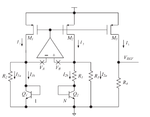
band.png

Now, i've done the math for the resistor and current values, assuming an ideal opamp.
Assume a standard 0.13um CMOS process that gives us CTAT 1.73mv/C and PTAT = 0.09 mv/C
CTAT/PTAT = 19.2 I chose 1:8 bjt ratio meaning R3/R1 = 9.24

I chose a Q1 - Q2 ratio of 1:8 so that gives us 0.0541 V around R1 (delta VBe = VT*ln(8))
For a 6uA current on that branch that would gives us an R1 ~9k
With R3/R1 ratio it gives us R3 = 83k.

Meaning the current over R3 = Va (Vbe) = Vb = ~0.7/83k = 8.4uA.

So, looking at the picture we have I2a = 8.4uA, I2b=6uA. This gives I2 = 8.4+6 = 14.4uA.


Now the questions.
If we assume 30ºC that gives Vbe of around 0.7 = Va = Vb. At this point what value do we expect at opamp output (mosfet gates)?
If the gates are driven by the opamp then I should scale their W/L so that the current I1 = I2 equals that value calculated before (14.4uA) right?


Thanks,
 

If the gates are driven by the opamp then I should scale their W/L so that the current I1 = I2 equals that value calculated before (14.4uA) right?
Right!

If we assume 30ºC that gives Vbe of around 0.7 = Va = Vb. At this point what value do we expect at opamp output (mosfet gates)?

Vsupply - |Vgs| , which is necessary to allow for the a.m. current and W/L. This voltage will be adjusted automatically due to the feedBack action.
 
Hi cr4zypt,


If we assume 30ºC that gives Vbe of around 0.7 = Va = Vb. At this point what value do we expect at opamp output (mosfet gates)?

I think your 'existential questions' are regarding how the circuit will work if both inputs to the Op Amp are the same for some reason.
If that happens, the output of the Op-Amp would be what ever its output common mode is. Now there are three possibilities.
  1. The output voltage is such that Vgs of the PMOS is MORE than expected. Then the current would be more, the Va and Vb would change(increase), and the output of the Op-Amp would settle to the correct value.
  2. The output voltage is such that the Vgs of the PMOS is LESS than expected. The the current would be less, the Va and Vb would change(decrease), and the output of the Op-Amp would settle to the correct value.
  3. The output voltage is just right. Well then there is no problem.

In real life there would be things like offsets and whatnot that will ensure that the Va ≠ Vb.

But the magic of negative feedback is such that it does not matter whether there is offset or not, the Output will always settle to the correct value(if designed properly!).


If the gates are driven by the opamp then I should scale their W/L so that the current I1 = I2 equals that value calculated before (14.4uA) right?

'Ideally' you don't even have to do this. The output of the Op-Amp would set the gate voltage such that it sets the correct value of current no matter what the size of the PMOS.

But of course in real life, if you size the PMOS like say 1/100, you might end up needing some massive Vgs to get the correct current! And you are limited by a bunch of things like Vdd and headroom and whatnot.

So you just size the PMOS to give this current with the Vgs determined by the output common mode of the Op-Amp. It is sort of a trade off between the Op-Amp design(what voltage range it has to handle) and the PMOS size(how big/small W/L).
 
I have a small problem to fix now.

It seems that the feedback network is highly unstable due to device mismatches. The only difference between N and P feedback loop is R1, about 10x smaller than R2=R3. Are there any advice on how to ensure feedback loops are stable, even in the presence of device mismatches? This at DC. I ran a few MCs and in some points my circuit wouldn't even work properly (the vref would have random values, generally close to 0v).
 

Bandgap Voltage Feedback Problem

And here I am again, this time with another problem.

**broken link removed**

The problem i'm facing right now is instability due to device mismatches.

From the picture you can see that the only difference between N and P loops is R1.
Now, in my case R1 is fairly small and about 10x smaller than R2=R3.

Running MonteCarlo simulations causes this small difference between feedback loops to become nearly non existent and placing my circuit in instability, meaning that it doesnt' work properly. The Vref if around 0V is those cases.

Is there any alternative to increasing the feedback diference without changing the resistor values? Since they are the ones that rule the weights of PTAT and CTAT
This instability is at DC, due to MonteCarlo mismatches.

Thanks,
 

Re: Bandgap Voltage Feedback Problem

From the picture you can see that the only difference between N and P loops is R1.
Now, in my case R1 is fairly small and about 10x smaller than R2=R3.

With such a big factor R3/R1, MC mismatch changes shouldn't generate large enough changes in the 2 feedback loops.

I think you have mixed-up the input polarity of the opAmp: the branch with R1 should feed the positive feedback loop, cf. with your own image above: View attachment 114802
 

Status
Not open for further replies.

Similar threads

Part and Inventory Search

Welcome to EDABoard.com

Sponsor

Back
Top