ghattasak
Member level 1
hello guys
I am working on a project: block matching using online adders and Sum of absolute difference computation
I have written the VHDL code and run the project fully on 3.8ns on altera cyclone V but i did not put any constraint on my input and output yet
I would like you if possible to check my coding style in the following files and note hints and guides and your opinion on how good or bad it is for future reference and projects.
the top level design is the block_add file
the olcomp is the online comparator used it has a large computational circuit I used a case statement to implement it is it ok?
as I noticed after implementing the comparator in the given way my clock increased from 3 to 3.8
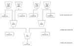
I have attached an image showing the circuit implemented in the block_add file
I have also a question regarding timing the unconstrained input and outputs on xilinx implementation I got a clock of 3ns without having to specify any constraints but altera requires them specified I have checked the timequest tutorial but did not understand on what to base my input and output timing constraints in addition is adding registers to inputs and outputs solves the problem?
please let me know of your opinion
thank you
I am working on a project: block matching using online adders and Sum of absolute difference computation
I have written the VHDL code and run the project fully on 3.8ns on altera cyclone V but i did not put any constraint on my input and output yet
I would like you if possible to check my coding style in the following files and note hints and guides and your opinion on how good or bad it is for future reference and projects.
the top level design is the block_add file
the olcomp is the online comparator used it has a large computational circuit I used a case statement to implement it is it ok?
as I noticed after implementing the comparator in the given way my clock increased from 3 to 3.8
I have attached an image showing the circuit implemented in the block_add file
I have also a question regarding timing the unconstrained input and outputs on xilinx implementation I got a clock of 3ns without having to specify any constraints but altera requires them specified I have checked the timequest tutorial but did not understand on what to base my input and output timing constraints in addition is adding registers to inputs and outputs solves the problem?
please let me know of your opinion
thank you
 I will recheck the tutorial and specify them a multi-cycle then my inputs are 64 - 2bit signals a start signal and a reset I did not check how will my input get in as it's a very large and annoying design part since my design is serial with parallel circuits I will need to input the first 64 - 2bit MSB first and so on till the 8th cycle into my adder tree. I was thinking of receiving the input data from fpga memory but did not research the different kind altera provides till now the inputs are given directly in a simulation test file