Continue to Site

Welcome to EDAboard.com

Welcome to our site! EDAboard.com is an international Electronics Discussion Forum focused on EDA software, circuits, schematics, books, theory, papers, asic, pld, 8051, DSP, Network, RF, Analog Design, PCB, Service Manuals... and a whole lot more! To participate you need to register. Registration is free. Click here to register now.

Vdd-1.2V voltage generation

Status
Not open for further replies.

viperpaki007

Full Member level 5
Full Member level 5
Joined
Jul 2, 2008
Messages
274
Helped
11
Reputation
22
Reaction score
8
Trophy points
1,298
Location
Finland
Visit site
Activity points
3,437
Hi,

I have a voltage source which varies from 4.2-3.7V. I need to generate voltage which is 1.2V less than vdd source and varies with Vdd source. For example, if Vdd=4.2V then output should be 4.2V-1.2V=3V and if Vdd=3.7V output should be 3.7V-1.2V=2.5V. Can somebody suggest what kind of circuit can be used.

regards
 

hi erikl,

i have never designed bandgap references so it is a bit difficult for me to design above circuit. Can you explain it a bit. Moreover, In my design kit bipolar transistors are not available. Is there any other circuit which only use MOS transistors.
 

Can you explain it a bit.
You got the schematic. W/L ratios depend on the process resp. PDK.

Moreover, In my design kit bipolar transistors are not available.
These are lateral PNPs; they don't need high B, B≈5..10 should be enough. If the process supports twin/triple well option, you could perhaps create your own devices. See your PDK, perhaps triple well lateral PNPs are characterized?

Is there any other circuit which only use MOS transistors.
You could use PMOS devices working in moderate/weak mode instead. Of course they will be considerably larger.
 

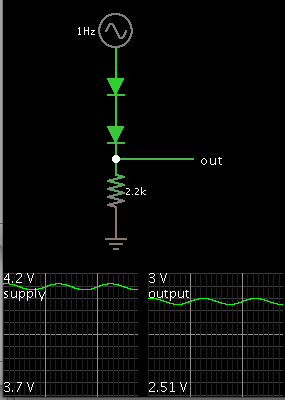
A silicon diode will drop about 0.6V. You may need to find the correct amount of current through it. You might need to test a few to find the correct type.

Two such diodes will drop 1.2V.

The scope traces show 3.7 to 4.2V being applied.

9181318100_1390339784.png
 

If you have the advantage of Somebody Else's Bandgap
then creating a high-side-referred image is easy. Take
a simple NMOS diff amp and drive a NMOS follower FET
from its output, loaded with (say) a 10Kohm resistor
and that point (load) fed back to null against VBG.
Now you have, out of the drain, a VBG/R(10K) current.

Throw that current at a VDD-returned equal construction
10K resistor, and there's your VDD-VBG reference. You
can rebuffer that if need be.

Caveats include background voltco if it's an implanted
resistor (junction isolated), and functionality at very low
VDD (buffer amp will need about VBG+VT before it can
work at all, and more to make full current fidelity) -
what happens when (say) VSS referred biases are up,
but VDD-referred are not?
 

Status
Not open for further replies.

Part and Inventory Search

Welcome to EDABoard.com

Sponsor

Back
Top