Continue to Site

Welcome to EDAboard.com

Welcome to our site! EDAboard.com is an international Electronics Discussion Forum focused on EDA software, circuits, schematics, books, theory, papers, asic, pld, 8051, DSP, Network, RF, Analog Design, PCB, Service Manuals... and a whole lot more! To participate you need to register. Registration is free. Click here to register now.

VCO design and sizing

Status
Not open for further replies.

jihrenee

Junior Member level 2
Joined
Aug 29, 2011
Messages
22
Helped
0
Reputation
0
Reaction score
0
Trophy points
1,281
Activity points
1,414
ask_vco.png
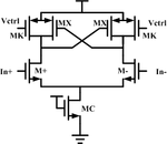
The image shown is a delay cell, where Vctrl is the control voltage. Where

MC: a current source work in triode region
MX: a negative resistance
MK: adjustable resistor
M+, M-: input pair

Connecting the delay cells in a loop will form a VCO.
Next, given Kvco, how can i size the MOS in this VCO to satisfy Kvco?
What i know so far is, i keep adjusting the size of MOS, run the simulation and draw the curve to calculate Kvco.
But strategy above is known as "hspice monkey" --- i'm just keep adjusting the size of MOS to ensure that the VCO will oscillate, and has enough swing.
Any direction to design a VCO?
 

What's wrong with "hspice monkey"? As soon as you have many second order effects and parasitics and transient specs, pure equation-based methods usually fail and simulation will play a key role in any sizing strategy.
 

Status
Not open for further replies.

Similar threads

Part and Inventory Search

Welcome to EDABoard.com

Sponsor

Back
Top