Continue to Site

Welcome to EDAboard.com

Welcome to our site! EDAboard.com is an international Electronics Discussion Forum focused on EDA software, circuits, schematics, books, theory, papers, asic, pld, 8051, DSP, Network, RF, Analog Design, PCB, Service Manuals... and a whole lot more! To participate you need to register. Registration is free. Click here to register now.

UPS repair

Gaber Mohamed Boraey

Full Member level 4
Full Member level 4
Joined
Feb 26, 2015
Messages
233
Helped
4
Reputation
10
Reaction score
11
Trophy points
1,298
Activity points
2,882
Hello

That board is inside 3kva ups , it’s inverter board
Take Dc input from 6 batteries in series , battery is 12v lead acid

Then goes to 4 mosfets high and low , every two are together, taking pulses from uc3845 pwm ic
Then goes to chopper then rectifiers then to ups inverter IGBT’s
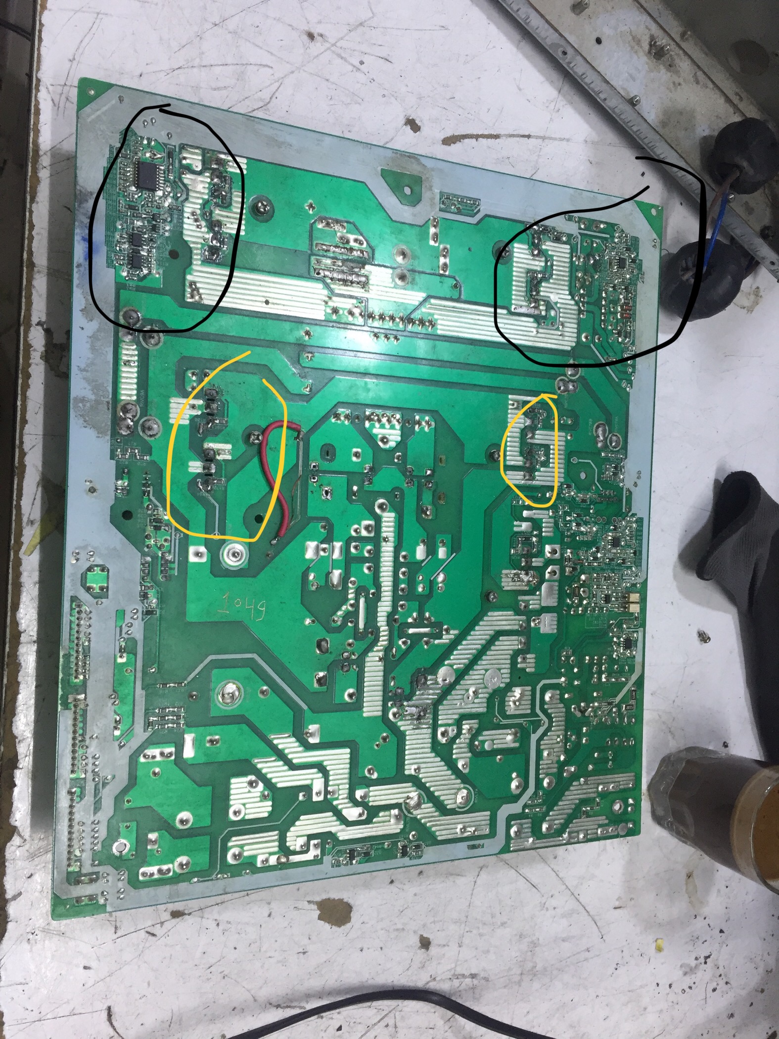
F95C5BA6-2513-40C1-ABA8-CF034A308D8E.jpeg


The black circles where the mosfets installed right and left the board
The yellows are the igbt’s

Here are the mosfets from other side of the board
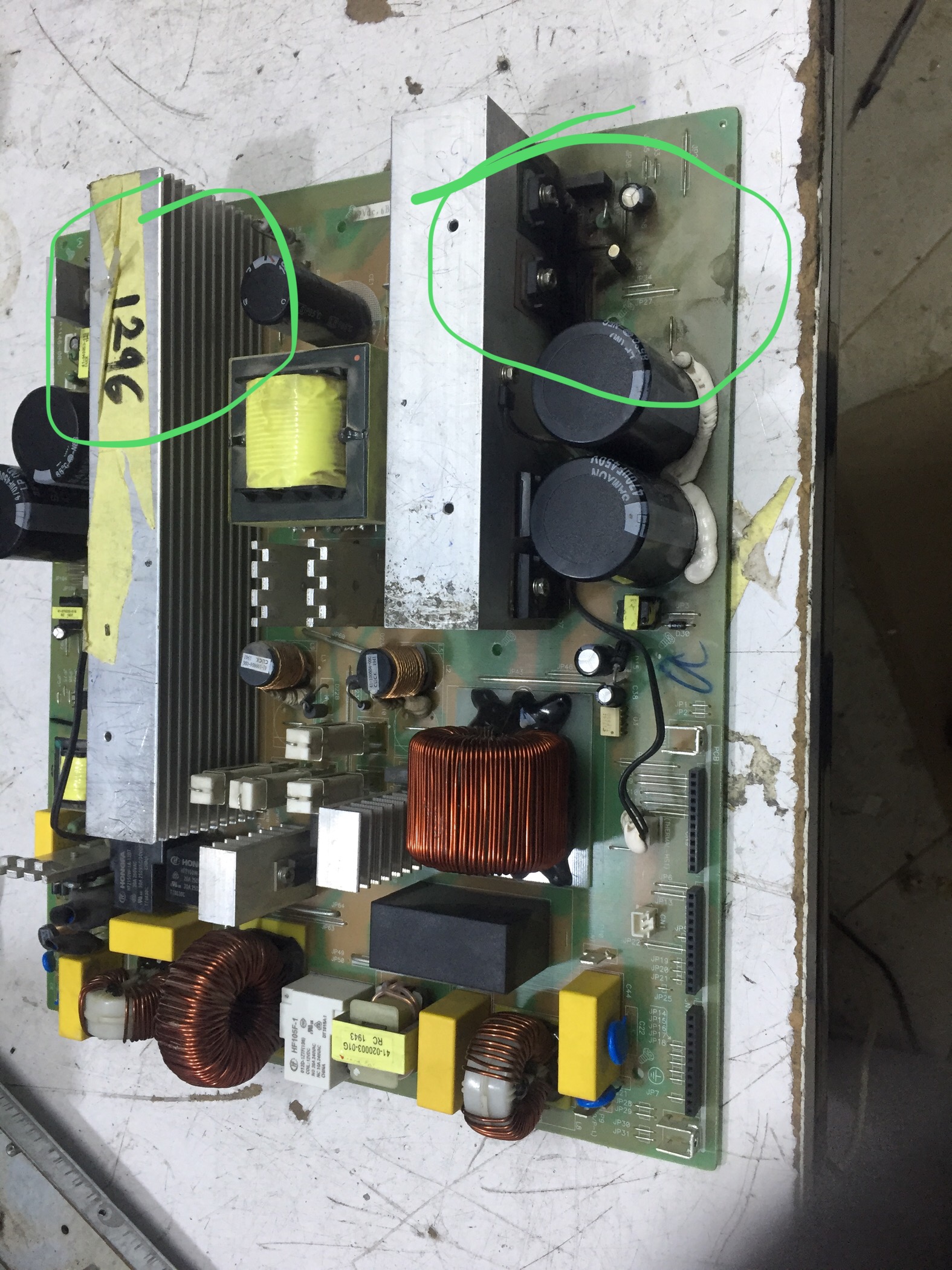
54161B52-4925-40F3-8803-EAFA824DFE1A.jpeg


This UPS came with many parts shorted, igbt’s, some igbt gate driver TL350, also mosfets, and some gates resistors
I’ve checked all and replaced , also found small chopper, this one beside the two big capacitors , open so I replaced with similar one “ but not sure if same coil turns “, can this be the problem?

When I tried to on the ups, damage occurred where are the mosfets, and one diode after the chopper
I’ve replaced and again damage happen
How you think is the problem?, I think it’s before the inverter, as every time the inverter try to start, damage happens
How you think?, do you have any suggest how solve?
 
If I were you, on the next repairing 'iteration' I would consider somehow opening the DC bus (battery, charger) and feed the 12v through an external power supply, current protected. Anyway, did you make the test after repair with a small or no load?
 
If I were you, on the next repairing 'iteration' I would consider somehow opening the DC bus (battery, charger) and feed the 12v through an external power supply, current protected. Anyway, did you make the test after repair with a small or no load?
Do you mean voltage injection? With 12v?
 
Yes...not to burn everything; its a usual procedure in cases like this, unless you have some better idea to put the inverter to work with a limited current, other than with the gigantic capacity of the lead acid battery; If it is capable of igniting a vehicle engine, imagine what it cannot do with a mere electronic circuit.
 
but where I feed this 12v?
There is no straight response, you need to perform some investigation there to find the suited part to disconnect and inject the external power supply.

for what the 12v?

You need to see the circuit working, or at least attempting to work to minimaly understand if the problem is on the logic side (PWM IC), in the power side (MOSFET, IGBT). A small current capacity power supply is able to, supply the logic side, but not with a current enought to heat a lot the switching devices...not necesssary to say that you don't need any load at this stage.
 
@andre_luis simply meant to replace the 12V with a current limited lab supply.

I recall generally whenever I tried to solve a mystery failure, I had to understand how it works.

How can that go wrong? Figure how it works.

Let's say you have IGBTs and FETs as parallel drivers for inversion at high dV/dt. We know the IGBT has a bipolar output which has the advantage of low pF output to reduce internal current dV/dt losses but have steady state higher losses for Vce(sat)/Ic = Rce can be as low as 1/Pd ohms or less but FETs have lower RdsOn but the disadvantage of higher Coss with lower RdsOn thus static losses but higher dynamic losses. The best of both devices could be (hypothetically) to turn on the IGBT turn on the FET to shunt RdsOn with Rce quickly but starting from a low Vce(sat).

What could go wrong? What are the failure mechanisms?

Well if the latency of Gate Drive to the IGBT was slower than the Gate Drive to the parallel FET resulting in a cascade of FET failures and if fused open then the IGBT.

How could the FETs fail if they are so much lower RdsOn than Rce. If they overheat from internal convection and conduction heating the BJT's which have a NTC will actually lower in Rce due to the diode law for -4mV/'C while FETs have a PTC effect which above a certain temperature will have thermal runaway that accelerates with load current.


How can be fault proof? This requires thermal monitoring, current and thermal limiting or OCP and OTP. Also when input voltage drops , input current must rise to supply demand load, so then there must be under-voltage protection or UVP. Finally timing of push-pull drivers must have a minimum dead-time or dead-band to prevent shoot-thru in the drivers from pre-driver and driver latency errors. FETs have a figure of merit (FoM) for a given Vds that is the product of Coss*RdsOn=Tau where lower is faster and thus less energy dissipated during transitions similar to all diodes and transistors but perhaps different. I once computed these in a spreadsheet using downloads of filtered searches from a major Disti site and plotted a scatter graph of Tau vs RdsOn above a required voltage. This can influence the dynamic losses and depends on the internal geometry and doping but latency may be harder to compare with dynamic loads and static losses.

1708017708127.png

1708017761212.png


Finally the closed loop regulation of output inverter voltage depends on closed and open loop margin and how it is compensated. Some regulators may require a minimum pre-load to remain stable and also require more Type III or D in the PID negative feedback to improve phase margin to avoid transient oscillations which are sure to upset parallel IGBT/FET drivers. The reason fro a preload is not obvious but if you analyze the stored energy in the reactance of the series loop with a very low RdsOn, you ultimately have an extremely high Q resonant LPF so choosing the damping factor is a tradeoff for no-load with a lossy RdsOn vs the static losses at full-load where the root{L/C} impedance is now damped by the parallel load resistance.

Wishful thinking is to find the actual schematics then simulate it in Simplis, MicroCap, LTpowerCAD, or whatever tools you want to learn.

This is just my hypothetical understanding of how your UPS inverter works. It's up to you to delve deeper and understand how your UPS works and what could go wrong with dynamic losses and steady state losses.

It's up to you to do the homework with some guidance from others.
 
How can be fault proof? This requires thermal monitoring,
Can not thermal monitoring, it happens in a moment that gets damage without even any loads
Do you think it can be some short circuit?, and so voltage injection can be a solution for discovery the faulty part?
 
Can not thermal monitoring, it happens in a moment that gets damage without even any loads
Do you think it can be some short circuit?, and so voltage injection can be a solution for discovery the faulty part?
Shootthru? What fails? p/n 's Gate drivers? p/n.
Do some analysis and give data, not words.
It's up to you to do the homework, not for us to dig for clues
 
Last edited:

LaTeX Commands Quick-Menu:

Similar threads

Part and Inventory Search

Welcome to EDABoard.com

Sponsor

Back
Top