matt11
Newbie level 4

- Joined
- Jun 22, 2012
- Messages
- 7
- Helped
- 0
- Reputation
- 0
- Reaction score
- 0
- Trophy points
- 1,281
- Activity points
- 1,362
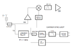
I am working on a carrier recovery design and have been experiencing issues. I have attached a block diagram of the design for reference.
The primary issue is that PLL#3 does not lock continuously. This PLL will intermittently lock and is displayed by the lock detect indicator pulsing on and off.
The general operation is: an unmodulated carrier is transmitted by another device and received at the antenna and designated F1. This signal is then down mixed to approx. 450 KHz. The 450 KHz signal is used as the oscillator input on PLL#3. PLL#3 controls a VCTCXO which is used to provide the appropriate reference clock for PLL/VCO#2.
In order to achieve the initial lock we are working on the premise that the VCTXO will be at a max or min frequency limit when PLL#3 is not locked due to the tuning output being railed high or low. The objective is to lock the VCTCXO to the device that transmits the unmodulated carriers TCXO.
Can anyone confirm the general theory/operation of this design is correct?
Thanks
The primary issue is that PLL#3 does not lock continuously. This PLL will intermittently lock and is displayed by the lock detect indicator pulsing on and off.
The general operation is: an unmodulated carrier is transmitted by another device and received at the antenna and designated F1. This signal is then down mixed to approx. 450 KHz. The 450 KHz signal is used as the oscillator input on PLL#3. PLL#3 controls a VCTCXO which is used to provide the appropriate reference clock for PLL/VCO#2.
In order to achieve the initial lock we are working on the premise that the VCTXO will be at a max or min frequency limit when PLL#3 is not locked due to the tuning output being railed high or low. The objective is to lock the VCTCXO to the device that transmits the unmodulated carriers TCXO.

Can anyone confirm the general theory/operation of this design is correct?
Thanks
