allennlowaton
Full Member level 5
Good day Guys...
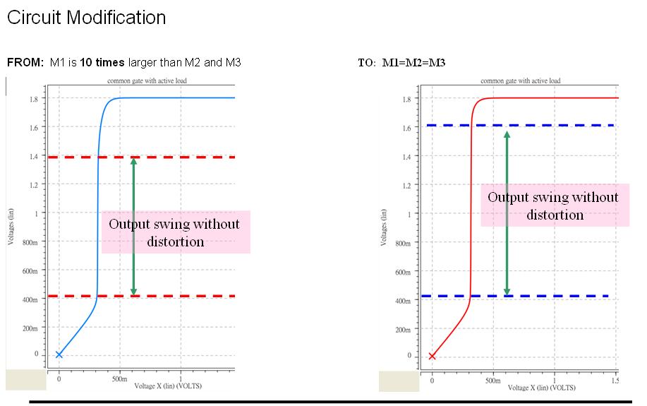
I'm doing a common gate right now..The load is a current source composed of 2 PMOS transistors..My driver transistor (where the input is delivered) has an aspect ratio 10 times as with the 2 PMOS. The Iref of the current source is 100uA with L=1u and W=10u.
At the transient analysis, as I increased the input from 1mV to 3mV...
The positive cycle swings LESS as compared with the negative cycle. What happen?
(according to ac analysis, the gain is 45dB)...
And also what keeps the positive cycle to stay stuck at 1.3V, why can't it reached 1.7v?
Please help me with this...
Below is the image of the wave..