FreshmanNewbie
Full Member level 6
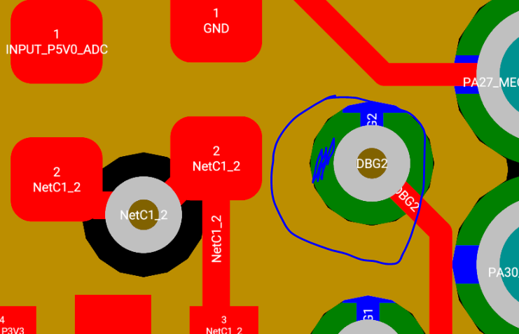
I've a PCB with 4 layers and trying to understand how the signals and vias in the layout are connected.
Layer 1 - Red colour signals
Layer 2 - Ground Plane (Yellow)
Layer 3 - Green
Layer 4 - Blue color signal

I want to understand the marked signal (DBG2) which is going from Layer 1 (Red) to Layer 4 (Blue). But why does it have an extra green circle around it?
And also, why NetC1_2 has a black void around it? The NetC1_2 net doesn't connect to anyother plane in the PCB.
Layer 1 - Red colour signals
Layer 2 - Ground Plane (Yellow)
Layer 3 - Green
Layer 4 - Blue color signal
I want to understand the marked signal (DBG2) which is going from Layer 1 (Red) to Layer 4 (Blue). But why does it have an extra green circle around it?
And also, why NetC1_2 has a black void around it? The NetC1_2 net doesn't connect to anyother plane in the PCB.