Continue to Site

Welcome to EDAboard.com

Welcome to our site! EDAboard.com is an international Electronics Discussion Forum focused on EDA software, circuits, schematics, books, theory, papers, asic, pld, 8051, DSP, Network, RF, Analog Design, PCB, Service Manuals... and a whole lot more! To participate you need to register. Registration is free. Click here to register now.

Understanding divide by 3 counter waveforms

Status
Not open for further replies.

ishan.dalal

Newbie level 5
Joined
Mar 6, 2014
Messages
10
Helped
0
Reputation
0
Reaction score
0
Trophy points
1
Activity points
66
Hey Guys,

I am not able to grasp the waveforms of divide by 3 counter where two flip-flops produce waveforms at half frequency but at quadrature phase relation.
Could anyone please explain me waveforms?

Thanks in advance !
 

Could you SHOW us the waveforms that you don't understand?

A schematic would be nice, too.
 

div_3.pngwaveform.png

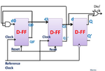
Hi, I have uploaded two images. One is counter design and second is waveform. I am unable to understand how Q1 and Q0 produce one clock pulse for every three clock pulses.
 

Did you notice the AND gate on the left is driven by the Qbar output of both flops? So when both flops are low they generate a pulse which then gets loaded into the first flop on the left, which then gets clocked into the middle flop. Once the pulse is gone it starts over again with the AND gate output going 1 again.
 

Hey I understand that. The thing I am unable to understand is the timing in waveforms. How Q1 and Q0 produce one clock pulse every 3 clock pulses?
 

Circuit can be better Understood assuming the Initial state of FF as "000".

- - - Updated - - -

Now You can analyze circuit clock by clock
clk0:= Initial state Q0 Q1 Q = 000,
Now Q0' Q1' are 1 hence d0=1.
clk1:= on this clock transition d0 is transferred to Q0. hence
Q0 Q1 Q = 100;
and Q0'=0 Q1'=1 so d0=0 and D1=Q0
clk2:= Now at this clock d1 is transferred to Q1 hence
Q0 Q1 Q = 010;
and Q0'=1 Q1'=0 and d0=0 again.
clk3:= now Q0 Q1 Q = 001;
and Q0'=1 Q1'=1 and d0=1.
now cycle clk4=clk1 hence it is repetition.
and this is how on every 3rd clock cycle(ofter their own high level) Q0 and Q1 becomes 1.


If it helped then hit help.
 

Got it, Thanks a ton !

Circuit can be better Understood assuming the Initial state of FF as "000".

- - - Updated - - -

Now You can analyze circuit clock by clock
clk0:= Initial state Q0 Q1 Q = 000,
Now Q0' Q1' are 1 hence d0=1.
clk1:= on this clock transition d0 is transferred to Q0. hence
Q0 Q1 Q = 100;
and Q0'=0 Q1'=1 so d0=0 and D1=Q0
clk2:= Now at this clock d1 is transferred to Q1 hence
Q0 Q1 Q = 010;
and Q0'=1 Q1'=0 and d0=0 again.
clk3:= now Q0 Q1 Q = 001;
and Q0'=1 Q1'=1 and d0=1.
now cycle clk4=clk1 hence it is repetition.
and this is how on every 3rd clock cycle(ofter their own high level) Q0 and Q1 becomes 1.


If it helped then hit help.
 

Status
Not open for further replies.

Part and Inventory Search

Welcome to EDABoard.com

Sponsor

Back
Top