Continue to Site

Welcome to EDAboard.com

Welcome to our site! EDAboard.com is an international Electronics Discussion Forum focused on EDA software, circuits, schematics, books, theory, papers, asic, pld, 8051, DSP, Network, RF, Analog Design, PCB, Service Manuals... and a whole lot more! To participate you need to register. Registration is free. Click here to register now.

TRIPLE WELL PROCESS (ISOLATING PWEL using DNWL)

Status
Not open for further replies.

ramitaco

Newbie level 1
Newbie level 1
Joined
Oct 30, 2013
Messages
1
Helped
0
Reputation
0
Reaction score
0
Trophy points
1
Visit site
Activity points
12
Hi I want to extract Layout of a DTMOS(ST45 nm). On DTMOS bulk is conected to Gate.

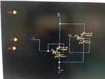
To isolate the bulk (Pwell) on a Nmos I am using DNW to provide vertical isolation and an Nwell guard ring to get a lateral isolation as figures depicted.
The main purpose of this is to get two isolated Pwell on the same DNW (it can be done, i checked on rule book).

The problem is that I am not able to pass the LVS test due to SCONNECT conflicts detected. foto 1a.jpgfoto 4.JPG
 

1. I can't see if your Nwell guard rings (also) are connected to VDD?
2. May be your DNW needs an extra (additional) connection to VDD?
 

Is it possible to have more than one isolated pwell (so different bulk connections for different NMOS devices) in a single deep nwell layer?
 

Is it possible to have more than one isolated pwell (so different bulk connections for different NMOS devices) in a single deep nwell layer?

Sure, why not? They should just have enough spacing, as not to risk BJT/SCR action between them.
An n+ guard ring connected to VDD (as tap of the Nwell resp. DNW) around the p-well should ensure this.
 
Sure, why not? They should just have enough spacing, as not to risk BJT/SCR action between them.
An n+ guard ring connected to VDD (as tap of the Nwell resp. DNW) around the p-well should ensure this.

ThankS Erikl .
May I avoid the n+ guard ring? This leads to a very large area occupancy due to the minimum area needed to the guard ring and to the distance needed beetwen two n+ guard ring. If i Connect deep nwell to vdd and use enough space (as explained by foundry rules) i think i generate two isolated Pwell (completely isolated one respect to the other ). Is it right?
 

I wouldn't actually risk to totally avoid it. If you really have to save this space, I'd draw at least an n+ guard line between the two pmos wells - at least if these are at different potential. You need an n+tap anyway, so it could well be between the two p-regions. That's a compromise between area saving and latch up risk prevention.
 

Status
Not open for further replies.

Part and Inventory Search

Welcome to EDABoard.com

Sponsor

Back
Top