Continue to Site

Welcome to EDAboard.com

Welcome to our site! EDAboard.com is an international Electronics Discussion Forum focused on EDA software, circuits, schematics, books, theory, papers, asic, pld, 8051, DSP, Network, RF, Analog Design, PCB, Service Manuals... and a whole lot more! To participate you need to register. Registration is free. Click here to register now.

Tri-state troubles with my basic CPU design (VHDL)

Status
Not open for further replies.

gavingt

Newbie
Newbie level 3
Joined
Dec 9, 2013
Messages
3
Helped
0
Reputation
0
Reaction score
0
Trophy points
1,281
Visit site
Activity points
1,350
Untitled.pngTestbench2.pngTestbench3.pngYou can see in the picture below the design our professor is having us implement. All the components simulate correctly and the design works perfectly on an FPGA board. But the testbench for the overall system is giving me tons of grief.

I'm getting this warning: Xst:2040 - Unit Microprocessor: 4 multi-source signals are replaced by logic (pull-up yes): A<0>, A<1>, A<2>, A<3>, but I don't know if that's a standard thing that Xilinx does or not. A(3:0) is the main bus going from the ROMs to the ALU.

I'm just trying to pass values through the ALU right now. As you can see in attached waveform, it's replacing every '0' with 'U's, but leaving the '1's intact (compare Aluout and hex_input_display).

Oh, and in addition to the components pictured, I made a somewhat sloppy display decoder for displaying results and debouncing two of the push button inputs.

Here's the overall VHDL file:


Code VHDL - [expand]
1
2
3
4
5
6
7
8
9
10
11
12
13
14
15
16
17
18
19
20
21
22
23
24
25
26
27
28
29
30
31
32
33
34
35
36
37
38
39
40
41
42
43
44
45
46
47
48
49
50
51
52
53
54
55
56
57
58
59
60
61
62
63
64
65
66
67
68
69
70
71
72
73
74
75
76
77
78
79
80
81
82
83
84
85
86
87
88
89
90
91
92
93
94
95
96
97
98
99
100
101
102
103
104
105
106
107
108
109
110
111
112
113
114
115
116
117
118
119
120
121
122
123
124
125
126
127
128
129
130
131
132
133
134
135
library IEEE;
use IEEE.STD_LOGIC_1164.ALL;
 
 
entity Microprocessor is
    Port ( clk : in  STD_LOGIC;   -- user-operated clock
            board_clk : in STD_LOGIC; -- clock from FPGA board
           Acctodatabus : in  STD_LOGIC;
           Loadacc : in  STD_LOGIC := '1';
           Invert : in  STD_LOGIC;
           Aonly : in  STD_LOGIC;
           Arithlogic : in  STD_LOGIC;
           hex_input : in  STD_LOGIC;
           reading : in  STD_LOGIC := '1';
           writing : in  STD_LOGIC := '0';
           rom_select : in  STD_LOGIC := '0';
           Aluout : out  STD_LOGIC_VECTOR (3 downto 0);
       hex_input_display : out STD_LOGIC_VECTOR (3 downto 0);
       DP : out STD_LOGIC;
       SSEG : out STD_LOGIC_VECTOR (6 downto 0);
       AN : out STD_LOGIC_VECTOR (3 downto 0)
              );
end Microprocessor;
 
architecture Structural of Microprocessor is
 
Component ALU is
    Port ( A : in  STD_LOGIC_VECTOR (3 downto 0);
           B : in  STD_LOGIC_VECTOR (3 downto 0);
           Cin : in  STD_LOGIC;
           Arithlogic : in  STD_LOGIC;
           Invert : in  STD_LOGIC;
           Aonly : in  STD_LOGIC;
           Y : out  STD_LOGIC_VECTOR (3 downto 0);
           Cout : out  STD_LOGIC
              );
end component ALU;
 
Component REG4 is
    Port ( A : in  STD_LOGIC_VECTOR (3 downto 0);
           IE : in  STD_LOGIC;
           CLK : in  STD_LOGIC;
           CLR : in  STD_LOGIC;
           Y : out  STD_LOGIC_VECTOR (3 downto 0)
              );
end component REG4;
 
Component DECODER_4 is
    Port ( A : in  STD_LOGIC_VECTOR (3 downto 0);
           EN : in  STD_LOGIC;
           YF : out  STD_LOGIC;
              YE : out  STD_LOGIC;
              YD : out  STD_LOGIC;
              YC : out  STD_LOGIC;
              YB : out  STD_LOGIC;
              YA : out  STD_LOGIC;
              Y9 : out  STD_LOGIC;
              Y8 : out  STD_LOGIC;
              Y7 : out  STD_LOGIC;
              Y6 : out  STD_LOGIC;
              Y5 : out  STD_LOGIC;
              Y4 : out  STD_LOGIC;
              Y3 : out  STD_LOGIC;
              Y2 : out  STD_LOGIC;
              Y1 : out  STD_LOGIC;
              Y0 : out  STD_LOGIC);                                                                                                                      
end component DECODER_4;
 
Component BUFFER4 is
    Port ( EN1 : in  STD_LOGIC;
           EN2 : in  STD_LOGIC;
           A : in  STD_LOGIC_VECTOR (3 downto 0);
           Y : out  STD_LOGIC_VECTOR (3 downto 0)
              );
end Component BUFFER4;
 
Component display_controller is
    Port ( board_clk : in STD_LOGIC;
              hex_input : in STD_LOGIC;   --BTN0 for selecting hex input value
              rom_select : in STD_LOGIC;  --BTN1 for selecting ROM
              Regout : in STD_LOGIC_VECTOR (3 downto 0); --receives final output from register
           SSEG : out STD_LOGIC_VECTOR (6 downto 0);
              rom_selected : out STD_LOGIC_VECTOR (3 downto 0);
              DP: out STD_LOGIC;   -- decimal point light indicates ROM 4 selected
              AN : out STD_LOGIC_VECTOR (3 downto 0);
           hex_input_display : out STD_LOGIC_VECTOR (3 downto 0));
end component display_controller;
 
signal A : STD_LOGIC_VECTOR (3 downto 0):= (others => '0'); -- main bus line A
signal B : STD_LOGIC_VECTOR (3 downto 0):= (others => '0'); -- B bus
signal and1out, and2out : STD_LOGIC;
signal Alu_to_Reg4_1 : STD_LOGIC_VECTOR (3 downto 0) := (others => '0'); -- connects ALU to Reg4_1
signal Reg4_2out : STD_LOGIC_VECTOR (3 downto 0); -- leaves outputs register, goes into display_controller
signal Reg4_3_to_Buffer_2 : STD_LOGIC_VECTOR (3 downto 0); -- connects Reg4_3 to Buffer_2
signal DECODER_4_out0 : STD_LOGIC; -- output 0 of decoder_4
signal DECODER_4_out1 : STD_LOGIC; -- output 1 of decoder_4
signal DECODER_4_out2 : STD_LOGIC; -- output 2 of decoder_4
signal DECODER_4_out3 : STD_LOGIC; -- output 3 of decoder_4
signal DECODER_4_outF : STD_LOGIC; -- output 
signal hex_input_display_signal : STD_LOGIC_VECTOR (3 downto 0) := (others => '0');
signal rom_selected_signal : STD_LOGIC_VECTOR (3 downto 0);
 
begin
 
hex_input_display <= hex_input_display_signal;
 
Aluout <= Alu_to_Reg4_1;
 
and1out <= DECODER_4_out0 and writing;
and2out <= writing and DECODER_4_outF; 
 
ALU_1: ALU port map (A => A, B => B, Cin => '0', Arithlogic => Arithlogic, 
                     Invert => Invert, Aonly => Aonly, Y => Alu_to_Reg4_1); 
REG4_1: REG4 port map (A => Alu_to_Reg4_1, IE => Loadacc, CLK => clk, CLR => '0', Y => B);
REG4_2: REG4 port map (A => A, IE => and1out, CLK => clk, CLR => '0', Y => Reg4_2out);
REG4_3: REG4 port map (A => A, IE => and2out, CLK => clk, CLR => '0', Y => Reg4_3_to_Buffer_2);
display_controller_1: display_controller port map(board_clk => board_clk, hex_input => hex_input, 
                      rom_select => rom_select, Regout => Reg4_2out, SSEG => SSEG, 
                             rom_selected => rom_selected_signal, DP => DP, AN => AN, 
                             hex_input_display => hex_input_display_signal);
BUFFER4_1: BUFFER4 port map (EN1 => Acctodatabus, EN2 => Acctodatabus, A => B, Y => A);
BUFFER4_2: BUFFER4 port map (EN1 => reading, EN2 => DECODER_4_outF, A => Reg4_3_to_Buffer_2, Y => A);
BUFFER4_3: BUFFER4 port map (EN1 => DECODER_4_out0, EN2 => reading, A => hex_input_display_signal,
                             Y => A);
BUFFER4_4: BUFFER4 port map (EN1 => DECODER_4_out1, EN2 => reading, A => hex_input_display_signal,
                             Y => A);
BUFFER4_5: BUFFER4 port map (EN1 => DECODER_4_out2, EN2 => reading, A => hex_input_display_signal,
                             Y => A);
BUFFER4_6: BUFFER4 port map (EN1 => DECODER_4_out3, EN2 => reading, A => hex_input_display_signal,
                             Y => A);       
DECODER_4_1: DECODER_4 port map (A => rom_selected_signal, EN => '1', YF => DECODER_4_outF,
                                 Y3 => DECODER_4_out3, Y2 => DECODER_4_out2, Y1 => DECODER_4_out1,
                Y0 => DECODER_4_out0);
 
end Structural;

 
Last edited by a moderator:

The ALU inputs aren't shown in the waveform, so we can only guess about the source of 'U' bits.

I don't know if your simulator is able to trace the source of 'U' signals, but you can do it manually. Displaying the ALU input signals would be a first step.

The 'U' bits may be related to the A multi-source problem. Apparently XST is applying a resolution function instead of flagging it as an error. In fact the warning is indicating a logic design error.

To avoid multi-source problems, you should guarantee that all drivers to bus A are mutually exclusive. That's not the case presently because Acctodatabus and reading are external signals that can be activated simultaneously.
 

Does Buffer4 create tristates? Does the Xilinx FPGA have internal tristates? If not, what should happen to them. Is your statement, "pull-up yes" a question? If the tool correctly handles it, it will be logic - such as a multiplexer or AND-OR tree.

What I have done is code it without tristates as an AND-OR tree. To do this, make the output of each Buffer4 a "0000" when it is not selected, and then "OR" all of the different sources of these together.
 

Does Buffer4 create tristates? Does the Xilinx FPGA have internal tristates?
I don't understand the question. The code is written as if Buffer4 has tristate outputs. Internal tristates can be used in code, but will be translated to muxes. The problem starts if the enable signals to individual drivers aren't mutual exclusive. Apparently the simulator has here a problem that doesn't exist in synthesized hardware.

I would lock "reading" against "Acctodatabus" to remove the multi-source problem.
 
The ALU inputs aren't shown in the waveform, so we can only guess about the source of 'U' bits.

I don't know if your simulator is able to trace the source of 'U' signals, but you can do it manually. Displaying the ALU input signals would be a first step.

The 'U' bits may be related to the A multi-source problem. Apparently XST is applying a resolution function instead of flagging it as an error. In fact the warning is indicating a logic design error.

To avoid multi-source problems, you should guarantee that all drivers to bus A are mutually exclusive. That's not the case presently because Acctodatabus and reading are external signals that can be activated simultaneously.

I've edited the full waveform diagram into my original post. I'm considering what I can do in reference to your last paragraph.


Does Buffer4 create tristates? Does the Xilinx FPGA have internal tristates? If not, what should happen to them. Is your statement, "pull-up yes" a question? If the tool correctly handles it, it will be logic - such as a multiplexer or AND-OR tree.

What I have done is code it without tristates as an AND-OR tree. To do this, make the output of each Buffer4 a "0000" when it is not selected, and then "OR" all of the different sources of these together.

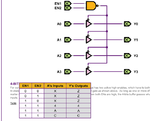
- The Buffer4 components do indeed create tri-states. I've included a picture
- I'm not the one to ask about Xilinx in general, but my understanding is that they no longer support internal tri-states signals. So they converted it into logic instead, which I think is what's going on in the other picture I've posted.
- The italicized line of text in my original post is the entirety of the warning message. "pull-up yes" wasn't commentary or anything.

RTL Schematic, Buffer4.pngbuffer4.png

- - - Updated - - -

I don't understand the question. The code is written as if Buffer4 has tristate outputs. Internal tristates can be used in code, but will be translated to muxes. The problem starts if the enable signals to individual drivers aren't mutual exclusive. Apparently the simulator has here a problem that doesn't exist in synthesized hardware.
I would lock "reading" against "Acctodatabus" to remove the multi-source problem.

OK, so what I did was to create two new signals, then replaced acctodatabus and reading in the port maps with the new signals.


Code VHDL - [expand]
1
2
AND_to_buffer_1 <= acctodatabus AND (NOT reading);
AND_to_ROMS <= reading AND (NOT acctodatabus);


Unfortunately, it had no effect. Perhaps I should do the same for the pairs "writing" and "reading" and "loadacc" and "acctodatabus"?

I should also note this other warning I've been getting, which I downgraded a while back from an error:

WARNING:place:1019 - A clock IOB / clock component pair have been found that are not placed at an optimal clock IOB /
clock site pair. The clock component <clk_BUFGP/BUFG> is placed at site <BUFGMUX_X1Y1>. The IO component <clk> is
placed at site <IPAD114>. This will not allow the use of the fast path between the IO and the Clock buffer. This is
normally an ERROR but the CLOCK_DEDICATED_ROUTE constraint was applied on COMP.PIN <clk.PAD> allowing your design to
continue. This constraint disables all clock placer rules related to the specified COMP.PIN. The use of this override
is highly discouraged as it may lead to very poor timing results. It is recommended that this error condition be
corrected in the design.
 
Last edited by a moderator:

I don't use Xilinx Xst, so unfortunately I don't know if warning 2040 appears regularly when internal tristates are converted to logic or only if the tristates involve potential multiple-driver conflicts. May be other Xilinx users can clarify the point.

The warnings are given by the synthesis tool and aren't directly related to simulation results. The reason why you get uninitialized signals in your simulation must be interrogated in the simulation itself. My assumption that the 'U' values are related to multi-driver problems is possibly wrong. It may be just regular behaviour due to missing signal initialization in simulation. I see that some signals are explicitely initialized to '0' in your design, but there may be others that propagate an 'U' state.

Occurrence of 'U' states is a common simulation mismatch case due to the fact that the default state of std_logic is 'U' while hardware registers can only take '0' or '1' state and have typically a power-on reset state of '0'.

As said, it should be always possible to find the source of 'U' by tracing through signals in the simulation.
 

Status
Not open for further replies.

Similar threads

Part and Inventory Search

Welcome to EDABoard.com

Sponsor

Back
Top