Continue to Site

Welcome to EDAboard.com

Welcome to our site! EDAboard.com is an international Electronics Discussion Forum focused on EDA software, circuits, schematics, books, theory, papers, asic, pld, 8051, DSP, Network, RF, Analog Design, PCB, Service Manuals... and a whole lot more! To participate you need to register. Registration is free. Click here to register now.

Transmission Line Calculator

Status
Not open for further replies.

SvenB

Junior Member level 1
Joined
Nov 28, 2014
Messages
15
Helped
4
Reputation
8
Reaction score
3
Trophy points
3
Location
Delft, The Netherlands
Activity points
137
Hi guys,

I made a MATLAB tool which can be used for characterizing printed transmission lines at microwave frequencies. The input of the tool looks as follows:
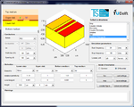
Screenshot.png

And it will give an output like this:
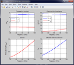
Screenshot2.png

It will give you the complex wavenumber, the characteristic impedance, effective dielectric constant and total losses. The total losses is a sum of ohmic losses, dielectric losses and radiation losses. This tool is quite powerful as there are no analytical tools or formulas available to calculate radiation losses, while these losses become really important when going to higher frequencies.

The available structures to analyze are:
1. Strip
2. Coupled Stripes
3. Microstrip
4. Coupled Microstrip
5. Stripline
6. Slotline
7. Coplanar Waveguide (CPW)

It also supports superconductive materials!

This is the stand-alone program directly from our group's website:
http://terahertz.tudelft.nl/Research/project.php?id=74&ti=27

Please give it a try and tell me if you find any bugs or missing any features!

Sven van Berkel
 
Last edited by a moderator:

Hi Sven,

this is great, thank you!

Can you give some background information on the calculation method?
From what I remember, there is some runtime version of Matlab available for those users who don't have a Matlab license?

Best regards
Volker
 

Hi Volker,

I am glad you like it. The MATLAB-tool uses a quasi-analytical approach. It sets up an electric field integral equation (EFIE) for the strip-type and continuity of magnetic field integral equation (CMFIE) for slot-type transmission lines. The excitation used is a delta-gap source in the middle of the line. The transmission lines are modeled by means of the Green's Functions for stratified media. With this integral equation we are looking for the poles in the spectrum which are resembling the propagating modes along the line. And these poles are then tracked by a first-order taylor expansion.

I am now also working on a new version that can account for surface-waves! There is also some background explanation in the Help-file of the GUI but if you have any other questions please don't hesitate to ask them!

Concerning some sort of "runtime version of MATLAB", I have never heard of it. You have experience with this? MATLAB is required as numerical integrations are performed.

Kind regards,
Sven
 
A compiled Matlab application can be in fact distributed and used without a Matlab license. Alternatively the program may work with GNU Octave, the free Matlab replacement.
 
  • Like
Reactions: SvenB

    SvenB

    Points: 2
    Helpful Answer Positive Rating
I found the Application Compiler in MATLAB. The first try is giving some errors in the program. However, give me some time and I'll will have a nice compiled version ready for you!
 
Hi SvenB,

This looks great - I'm looking forward to the addition of surface wave modes.

I see you have the excitation set up as common or differential, are you planning on generalizing this for a multi-modal environment?

Thanks for sharing your hard work.
 

I'm looking forward to the addition of surface wave modes.

Hi PlanarMetamaterials, only the first surface wave mode will be accounted for. These are:
1. Strip => TE0
2. Coupled Stripes => TE0
3. Microstrip => TM0
4. Coupled Microstrip=> TM0
5. Stripline => TM0
6. Slotline => TM0
7. Coplanar Waveguide (CPW) => TM0

The two dielectric slabs can be characterized until an electrical height of lambda_d/2 where lambda_d is the wavelength in the dielectric. After this height, the power going into a surface-wave is already comparable with radiation into an infinite dielectric. Therefore, if you will have structures with a dielectric slab larger than lambda_d/2, you should model it as an infinite dielectric.

I see you have the excitation set up as common or differential, are you planning on generalizing this for a multi-modal environment?

I am not sure if I understand your question correct, but the spectrum, of a CPW for example, will show me two poles; one pole for the common excitation and one pole for the differential excitation. These are the two modes the user can choose to track. For other structures, only the main propagating mode will be tracked.

Kind regards,
Sven van Berkel
 

I compiled a standalone version of the program. It is attached to this message. It seems that it works properly. Check it out and let me know what you think!

Hi Sven,

I downloaded the standalone version and it works fine. There is some delay after starting the program where nothing seems to happen and I was wondering if the start failes, but obviously it was just delay from loading all the libraries in the background.

Some comments and ideas from an RFIC guys's perspective

- Your code seems to simulate with zero thickness. This is fine for wide flat metal (typical PCB case) but for on-chip cases the metal height becomes relevant. It changes loss for microstrip and it changes capacitance between metals for coupled lines and coplanar.

- It seems that we can edit parameters, but keep the old material text label that no longer applies?

- You could add SiO2 as lower slap material, which is very common as inter-metal dielectric in RFIC stackups. Permittivity is usually specified between 3.9 and 4.2, with small or zero loss tangent.

- You have included silicon as a dielectric with loss tangent. The bulk silicon that we have as bottom medium isn't accurately described by tand, because it has relevant (DC) conductivity. Typical values are in the range 1 .... 10S/m but it depends on the actual technology.

Best regards
Volker
 

I really appreciate your input so that the program can be improved.

- Your code seems to simulate with zero thickness. This is fine for wide flat metal (typical PCB case) but for on-chip cases the metal height becomes relevant. It changes loss for microstrip and it changes capacitance between metals for coupled lines and coplanar.

Indeed, the metals are simulated with zero-thickness with a surface-impedance assuming that the metal is electrically thick (t >> skindepth). A change in the surface impedance can be accounted for, in the case of a finite thickness, which I will implement in a future version. A change in field distribution however, and thus capacitance, cannot be accounted for unfortunately.

- It seems that we can edit parameters, but keep the old material text label that no longer applies?
Yes, that's true. The labels are there in order to load quickly some pre-programmed settings.

- You could add SiO2 as lower slap material, which is very common as inter-metal dielectric in RFIC stackups. Permittivity is usually specified between 3.9 and 4.2, with small or zero loss tangent.
I will add it!

- You have included silicon as a dielectric with loss tangent. The bulk silicon that we have as bottom medium isn't accurately described by tand, because it has relevant (DC) conductivity. Typical values are in the range 1 .... 10S/m but it depends on the actual technology.
This can be implemented easily. That may be nice to add in the future.

Kind regards,
Sven van Berkel
 

Hi Sven,

thanks again for this sharing project, and for your fast response!

Indeed, the metals are simulated with zero-thickness with a surface-impedance assuming that the metal is electrically thick (t >> skindepth).

Ok, that's expected. One comment on that: If you simulate the conductor as a thin sheet and calculate the equivalent surface impedance, you need to make an assumption if there is skin current only on one side (e.g. bottom) or both sides (top and bottom). Both cases exist, and anything in between. In microstrip the current is mostly on the bottom side of the conductor, whereas in stripline it is symmetric on both top and bottom side, resulting in two skin sheet in parellel. So the surface impdances mapped onto the conductor is different, depending on the actual field distribution for that conductor configuration.

A change in the surface impedance can be accounted for, in the case of a finite thickness, which I will implement in a future version. A change in field distribution however, and thus capacitance, cannot be accounted for unfortunately.

Yeah, I was mostly looking for the change in field distribution from finite thickness of the conductors. But I understand that's rather tough. The Sonnet solver approximates thick metal by stacking multiple thin sheets, but it might take many sheets in some cases, depending on geometry and skin depth.

Yes, that's true. The labels are there in order to load quickly some pre-programmed settings.

To avoid confusion with text label and value no longer matching: How about an explicit "user defined" setting, or alternatively take out the predefined material name when the user changes the values?

Best regards
Volker
 

If you simulate the conductor as a thin sheet and calculate the equivalent surface impedance, you need to make an assumption if there is skin current only on one side (e.g. bottom) or both sides (top and bottom).
This is actually discussed in the Help document provided with the program and good described by the paper of Rautio mentioned in the Bibliography of the Help document (This paper described the model in Sonnet). Indeed at this point the program does not account for this. I was thinking by implementing this by looking at the ratio of the dielectric constants of the slab to estimate the ratio between the top and bottom current and with that alter the effective surface impedance. What do you think?

To avoid confusion with text label and value no longer matching: How about an explicit "user defined" setting, or alternatively take out the predefined material name when the user changes the values?
Sure I agree with you, I will take care of it.

Anyways, new versions are online at the MATLAB File Exchange. There were problems with Matlab R2014b, which are resolved now. There are now three possibilities to run the program:
1. Stand-alone program (Requires free MATLAB Compiler Runtime but doens't require MATLAB license)
2. Matlab-App
3. Directly from the .m-files.

I am looking forward to new suggestions!

Sven
 

I am not sure if I understand your question correct, but the spectrum, of a CPW for example, will show me two poles; one pole for the common excitation and one pole for the differential excitation. These are the two modes the user can choose to track. For other structures, only the main propagating mode will be tracked.

I was thinking of conductor-backed dielectric slabs, which when combined with some of your waveguides can support three TEM modes (for example, CB-CPW). I imagine this would just appear in your solver as an additional pole.

Just a thought, thanks again!
 

This is actually discussed in the Help document provided with the program and good described by the paper of Rautio mentioned in the Bibliography of the Help document (This paper described the model in Sonnet). Indeed at this point the program does not account for this. I was thinking by implementing this by looking at the ratio of the dielectric constants of the slab to estimate the ratio between the top and bottom current and with that alter the effective surface impedance. What do you think?

Hi Sven,

yes I was coming from the Sonnet perspective (have done support for them for many years) and the Jim Rautio papers on this topic are what I would reference as well. I don't know if your dielectric constant ratio is the ideal way to go, because even a microstrip in air would have more current at the bottom side. Maybe just do it like Sonnet: use the pessimistic case and nobody will complain if measured loss is too low ;-)

Best regards
Volker
 

Unfortunately I cannot upload .exe files to the MATLAB File Exchange. This means that for now only the MATLAB-app will be uploaded to the file exchange. However, when the program is steady and also includes the first surface-waves I will develop the stand-alone version and upload it directly to the server of the university.

If someone really wants an updated version of the stand-alone program, just write a PM and I will send it to you personally.
 
Status
Not open for further replies.

Part and Inventory Search

Welcome to EDABoard.com

Sponsor

Back
Top