Continue to Site

Welcome to EDAboard.com

Welcome to our site! EDAboard.com is an international Electronics Discussion Forum focused on EDA software, circuits, schematics, books, theory, papers, asic, pld, 8051, DSP, Network, RF, Analog Design, PCB, Service Manuals... and a whole lot more! To participate you need to register. Registration is free. Click here to register now.

Transistor switch mode - explanation needed

Status
Not open for further replies.

jayce3390

Full Member level 6
Joined
May 22, 2007
Messages
351
Helped
29
Reputation
58
Reaction score
21
Trophy points
1,298
Activity points
3,287
Transistor switch mode

Hi all,

I performed a transient simulation of a basic MOSFET transistor in switch mode. The test set-up is described in the picture with simulated curves VDS and VGS.

I concluded, the more the drain resistor is high the more VDS is high.

Could you explain me why?
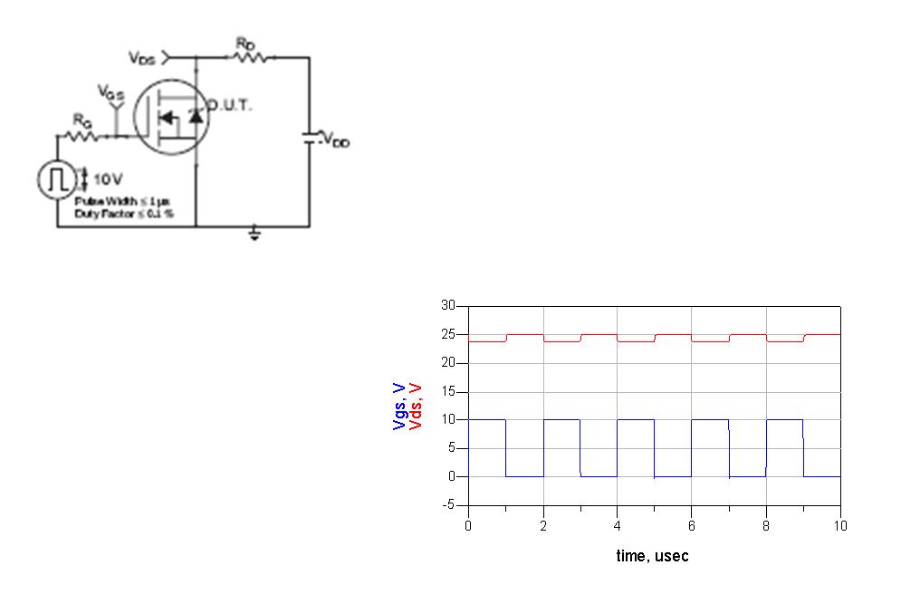
 

Transistor switch mode

If you look at the characteristics of a MOSFET

https://en.wikipedia.org/wiki/File:IvsV_mosfet.png

you will see that the "linear region" is fairly straight from the origin. So as you increase the voltage the current increases proportionally, looking like a resistor. If you apply a lot of voltage the current limits - you are in to the saturation region. Here the transistor looks like a current source.

So, if you take V/I to calculate a resistance, yes, V/I is higher at higher Vds. It is not really behaving like a resistor any more. It has "saturated".

Be careful with the "saturation" terminology. With a bipolar (NPN or PNP) transistor, saturation means something totally different!

Keith.
 

Re: Transistor switch mode

thank you keith1200rs.

We are talking about different drain resistor. I was referring to RD on the schematic I posted, not internal drain resistance of the MOSFET.

I understand IV curves you mentionned and differences between ohmic region and saturation region, but I don't know if you can explain my case with IV curves
 

Re: Transistor switch mode

jayce3390 said:
thank you keith1200rs.

We are talking about different drain resistor. I was referring to RD on the schematic I posted, not internal drain resistance of the MOSFET.

I understand IV curves you mentionned and differences between ohmic region and saturation region, but I don't know if you can explain my case with IV curves

Sorry, I don't understand the question then. The graph you show has a gate voltage pulsing from 0V to 10V. I don't know what the transistor is or the resistor, but what happens is the transistor turns on and pulls the voltage on its drain down from 25V (presumably your voltage source voltage) to around 24V. That is what I would expect. My guess is that the resistor you have in the drain is quite small so the transistor cannot pull the drain down very low.

Could you try to rephrase what it is that puzzles you and I will try to understand?

Keith.
 

Re: Transistor switch mode

My guess is that the resistor you have in the drain is quite small so the transistor cannot pull the drain down very low.

This is exactly the point I want to understand. RD resistor is setting the biasing point of the MOSFET on his IV curves? Is it something like that?

Assuming VDS is always 25V, If I increase RD, my biasing point will "go up" on the IV graph?

Thank you for your comment.
 

Re: Transistor switch mode

Arrrh. I just posted a long reply and it disappeared. I will try again.

RD is the load resistor. There is no "bias point" as such. The transistor is either on or off. I am probably going to confuse you even more, but you probably need to understand "load lines".

The attached pdf shows a simulation similar to yours, I think. I have used a 10V gate pulse and a 1ohm and 10ohm load resistor (RD in your diagram, R1 in mine). With a 1 ohm resistor the drain gets down to around 21.5V. With a 10 ohm resistor it gets down to around 4V.

To understand what is happening you need to look at the MOSFET characteristics. In the attached GIF I have plotted just one of the normal curves of Id versus Vds - for a Vgs of 10V - the gate voltage we are using. It is the red line. Hopefully you recognise it as one of the set of curves normally shown for MOSFETs.

The "load lines" I have plotted are for the 1 ohm and 10 ohm loads. The 10 ohm one starts at Vds=0 and Ids=2.5A. This is the condition if the MOSFET could turn on with zero resistance - the current would be 2.5A. The other end of the load line is at Id=0, Vds=25. This is the condition where the MOSFET is turned off. The actual operating point when the transistor is turned on will be where the load line crosses the MOSFET characteristics (the red line). This is at Vds=4V, Id=2.1A which is the same as the pulsed results.

the 1 ohm load line is trickier to draw because it needs to cross the Y axis at 25A (1 ohm across 25V) but I have approximated. The intersection of that line and the MOSFET characteristics is at around 21V. Again, the same as the pulse simulation.

I hope that helps and doesn't confuse you even more!

Keith.
 

    jayce3390

    Points: 2
    Helpful Answer Positive Rating
Re: Transistor switch mode

thank you very much, very clear.
 

Status
Not open for further replies.

Part and Inventory Search

Welcome to EDABoard.com

Sponsor

Back
Top