Continue to Site

Welcome to EDAboard.com

Welcome to our site! EDAboard.com is an international Electronics Discussion Forum focused on EDA software, circuits, schematics, books, theory, papers, asic, pld, 8051, DSP, Network, RF, Analog Design, PCB, Service Manuals... and a whole lot more! To participate you need to register. Registration is free. Click here to register now.

transistor as diode clamp

Status
Not open for further replies.

fm101

Member level 5
Joined
Apr 13, 2020
Messages
81
Helped
1
Reputation
2
Reaction score
4
Trophy points
18
Activity points
591
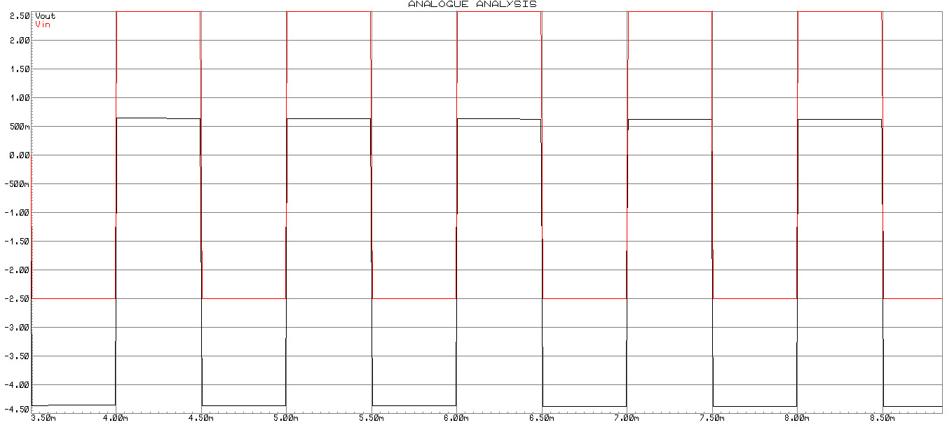
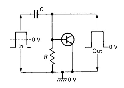
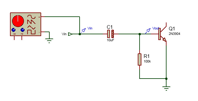
I tried the following circuit simulation in Proteus where transistor is used clamp the input voltage -2.5V to 2.5V to 0V to 5V but I am not getting the expected output voltage as shown in the graph. Why is it not working and how do I choose the capacitor and resistor values?
1.jpg


4.jpg


3.jpg
 

Solution
I understand the problem differently.

You want to clamp negative voltage but post #1 circuit clamps positive voltage. Wrong transistor polarity.

After flipping the polarity you'll get -0.7/4.3 V pulse. If you want ideal 0/5V output, a more complex circuit is required.
you need a resistor above R, 2k0 base to RHS of C, and Ritself should be 470 ohm, then collector goes straight up to RHS of C - this will give you a 2v5 clamp ...
--- Updated ---

you can scale these values also, e.g. 4k7 & 20k
 

you need a resistor above R, 2k0 base to RHS of C, and Ritself should be 470 ohm, then collector goes straight up to RHS of C - this will give you a 2v5 clamp ...
--- Updated ---

you can scale these values also, e.g. 4k7 & 20k
don't understand what you mean, R1 should be 470Ohm? I tried this and not working. what do you mean by 2k0 base to RHS(Right Hand Side) of C?
 

I'm sorry if you can't under stand simple instructions, there must be 2 resistors, the extant one shown must be 470 ohm, and the other needed one is from the base to the collector, i.e. the RHS of the cap, AND the collector must connect to the RHS of the cap too ....
 

I'm sorry if you can't under stand simple instructions, there must be 2 resistors, the extant one shown must be 470 ohm, and the other needed one is from the base to the collector, i.e. the RHS of the cap, AND the collector must connect to the RHS of the cap too ....
do you mean like this?
5.jpg
 

I understand the problem differently.

You want to clamp negative voltage but post #1 circuit clamps positive voltage. Wrong transistor polarity.

After flipping the polarity you'll get -0.7/4.3 V pulse. If you want ideal 0/5V output, a more complex circuit is required.
 

Solution
I understand the problem differently.

You want to clamp negative voltage but post #1 circuit clamps positive voltage. Wrong transistor polarity.

After flipping the polarity you'll get -0.7/4.3 V pulse. If you want ideal 0/5V output, a more complex circuit is required.
I got the circuit drawing from here:https://www.nutsvolts.com/magazine/article/bipolar_transistor_cookbook_part_1
and it says the output is 0V to 5V for input -2.5V and 2.5V which seems not be the case....am i right?
 

you missed out this bit : " AND the collector must connect to the RHS of the cap too .... "

you kinda have to follow all the instructions - not just pick and choose ....
--- Updated ---

do not connect the base to the cap ....
 

Hi,

I find the informations given on the site a bit misleading.

For sure one can just use BE of a BJT as a diode.
But this gives just a "weak" diode.

It´s far better to use the collector, too.

Also the description/explanation is not good.

***
If you want to get 0V/5V from a -2.5V/+2.5V input you need some active device.
Otherwise you always get about 0.6V offset. I.e: -0.6V / +4.4V output

***
To get -0.6V/+4.4V you just need a diode and a capacitor ( no BJT, no resistor.)
Diode: Anode to GND, cathode to output
capacitor: one side input, other side output

Mind: this all only works with very high ohmic load, rather low ohmic input, and the capacior needs to fit for freqeuncy and load resistance.

Klaus
 

Something like this :

Use R's to level shift (eliminate C, make DC coupled), followed by G = 2 RRIO OpAmp :

1667039045185.png


1667038780104.png


Regards, Dana.
 
Last edited:
Transistor as diode is neither weaker or stronger than regular diode, I think. CB diode has higher breakdown voltage than EB, in so far preferred. The problem with Fig.7 schematics in the link is however that both have wrong polarity.
 

The root question is, are you trying to make a logic signal from an offset input, or are you trying to "clamp" as you say.

The two roles want different details.
 

Hi,
Transistor as diode is neither weaker or stronger than regular diode, I think. CB diode has higher breakdown voltage than EB, in so far preferred.
I guess there is a misunderstanding. I did not mean to use CB diode.
I meant BE to control the BJT, while the "big" current runs through the collector.
Thus - due to hFE of the BJT - there is a steeper V-I rate.

Like usually when a BJT as temperature sensor is used: Emitter to GND, and not only B is used but (B+C) short circuited.

In the schematic of post#2 the collector is unused.

Klaus
 

The link you are reading basically breaks down the bipolar transistor into 2 discrete diodes which are not the same size and thus have different bulk resistance and voltage rise above 500 mV with current.

I might assume your sig. gen. is 50 Ohms source and thus current limited with (2.5V-0.63) / 50 = 37.4 mA
You might expect the collector to draw 10x the base current at the rated Vce(sat), but in your case the collector is not the output.

The base is the output.

But by connecting the base to the collector, you now boost the current gain if there is a load pulled up to some Vcc and thus affect the output saturation voltage rise on the collector.

THeir diagram on the right uses the NPN (sort of backwards) by swapping collector and emitter to show the voltage rise is roughly Vec = Vbe again with the standard voltage generator = 50 ohms which allows voltage divider relationship with the diode resistor being much smaller with 37 mA. Thus 630 mV. Typically the small signal diodes are about the same up to 500 mV to 600 mV then differ based on the chip power rating and bulk resistance.


1667061100366.png


The above adds a series cap to reduce the risk of burning out the base and a base to 0V to discharge the cap. But with care, these are not necessary.

Disregard the actual diode voltage which is based on some model. but this shows the same as above and what you got on Proteus except you got a value of 630mV based on some other model.

1667062404348.png


Next

Now the better rectifier using a transistor uses Vbe=Vce which is commonly used inside bipolar IC's for a bipolar clamp.

The reversed NPN at the bottom might not have any current gain ~ 1 . Notice just that the 671 mV is lower due to the current gain from a lower bulk resistance than just the Vbe when saturated. Don't analyze the values too much yet.

But remember that 1mA @ 600 mV is a better than saying all diodes are 0.7V. (due to the variation in bulk Rs that becomes significant as current rises > 1mA or so.

1667062525832.png
 

Hi,

As far as i understand the OP does not need a 2.5V clamp.
He rather needs a 0V / 5V clamp.

But the circuit is what I meant in post#13.


Klaus

Added:
A simple 0V/5V clamp could be a zener.
 

and for clamping both ways for a bi-polar input ( & output signal )

1667091159269.png

--- Updated ---

@FvM - I see your point - re-reading post #1 it appears he/she wants a -2v5 to 2v5 amplifier to 0 - 5V

i.e. -2v5 in = 0v out and +2v5 in = 5V out .... a buffer / amplifier not so much a clamp ...
--- Updated ---

Yes - in fact "clamp" is a bt of a misnomer for " DC restorer " circuit as follows:

1667091537600.png


so +/- 2v5 turns into 0 - 5V, best to use a low Vf schottky, and make sure the source can supply the required currents ....
--- Updated ---

the R can be 1Meg or larger to give a decent time constant ....
 
Last edited:

and for clamping both ways for a bi-polar input ( & output signal )

View attachment 179414
--- Updated ---

@FvM - I see your point - re-reading post #1 it appears he/she wants a -2v5 to 2v5 amplifier to 0 - 5V

i.e. -2v5 in = 0v out and +2v5 in = 5V out .... a buffer / amplifier not so much a clamp ...
--- Updated ---

Yes - in fact "clamp" is a bt of a misnomer for " DC restorer " circuit as follows:

View attachment 179415

so +/- 2v5 turns into 0 - 5V, best to use a low Vf schottky, and make sure the source can supply the required currents ....
--- Updated ---

the R can be 1Meg or larger to give a decent time constant ....
so you did not read my 1st post? I'm sorry if you cannot understand simple diagram that has been posted, let alone the problem described in words.
1-jpg.179378


I tried your solution 3 4 times but now I know why it was not working.

Turns out the correct way to use the transistor is as follows.(hinted by the Positive Clamper circuit with diode posted above).
2.jpg


The output is nearly 0V to 5V, except for the ~600mV as indicated in the graph below. This is the Vbe junction voltage. Is there way to up lift this 600mV so that the lower end is at 0V?
3.jpg

--- Updated ---

I understand the problem differently.

You want to clamp negative voltage but post #1 circuit clamps positive voltage. Wrong transistor polarity.

After flipping the polarity you'll get -0.7/4.3 V pulse. If you want ideal 0/5V output, a more complex circuit is required.

Transistor as diode is neither weaker or stronger than regular diode, I think. CB diode has higher breakdown voltage than EB, in so far preferred. The problem with Fig.7 schematics in the link is however that both have wrong polarity.

FvM has been mentioning the problem time to time and I just happened not to go through it. Although I went through the solution by Easy Peasy with the diode solution, FvM has first hinted out the problem so I am marking his answer as solution.
--- Updated ---

I understand the problem differently.

You want to clamp negative voltage but post #1 circuit clamps positive voltage. Wrong transistor polarity.

After flipping the polarity you'll get -0.7/4.3 V pulse. If you want ideal 0/5V output, a more complex circuit is required.
what additional circuit is required if I wanted 0/5V output? this is just interesting to me...
 
Last edited:

the original post was wrong:
1667115057635.png

as the output cannot go above 1 x Vbe, i.e. 0.6V approx

also clamp is a bad descriptor - Dc restorer is the correct label, as it is a level shifter.

Clamp circuits are per the 1st two I posted.

A simple internet search would reveal all the answers you apparently require.

Any way - you now have your answers
 

Hi,
so you did not read my 1st post? I'm sorry if you cannot undgerstand simple diagram that has been posted, let alone the problem described in words.
My - hopefully - objective point of view.
In post#1 we see a schematic that does not match the textual description.
Not your fault, because i'd say the informations given on the internet site are rather confusing maybe even wrong.
But also not our fault. If we see text that does not match the schematic we do not know which information we can rely on.

(hinted by the Positive Clamper
Indeed it's a negative clamper. It limits the negative voltage to about -600mV.
It does not care about positive voltage. It does not prevent the output to be +20V for example. Not sure whether this may cause a problem for your application or not.

*****
But a big problem is that we don't know what's your true target.
Is it a more theoretical school project with more 'idealistic" signals and devices.
Or is it a real probkem with real signal and realistic parts.
Frequency is totally unknown. Nor duty cycle. Nor whether this is a continous signal, or signal bursts or maybe a one shot.
All has some influence on a suitable solution.

So we don't need what to focus on.

In my decades of designing professional electronics I never had the problem to "DC shift" a digital signal while maintaining the levels in the 100mV range. I don't know what's the use case for your problem.

Klaus
 

Status
Not open for further replies.

Similar threads

Part and Inventory Search

Welcome to EDABoard.com

Sponsor

Back
Top