Continue to Site

Welcome to EDAboard.com

Welcome to our site! EDAboard.com is an international Electronics Discussion Forum focused on EDA software, circuits, schematics, books, theory, papers, asic, pld, 8051, DSP, Network, RF, Analog Design, PCB, Service Manuals... and a whole lot more! To participate you need to register. Registration is free. Click here to register now.

Transfert function of complex polyphase filter: simulation gain issue

Status
Not open for further replies.

Chr's

Junior Member level 1
Joined
Sep 26, 2014
Messages
16
Helped
0
Reputation
0
Reaction score
0
Trophy points
1
Visit site
Activity points
121
Hi,
iḿ currently work on plyphase filter.
I arrive to trace the correct frequency curve, where the cut-off frequency fit with the theory, but the gain.
I've a difference of 3 dB (more) with the theory.

So my question is:
Like 3dB=√2, when the calculator does the modul of I+jQ, the magnitude of I and this od Q are equal so the addition give twice the magnitude, so when de module is computed may be i've to divide by 2.
Like |I+jQ| =√((I²+Q²)/2)
= √(I²+Q²)/√2
= 20log(√(I²+Q²))-20log(√2)
= 20log(√(I²+Q²))-3

=> and I get my 3dB less and fit with the theory.

If I'm wring, anyone have an idea on the reason of 3dB more compare to the theory ?

Thanks in advance for your help.
 

Hi,
It's a Tow thomas polyphase filter diffrential with current input, so my gain is dB(V/mA).
 

Hi,
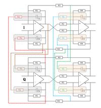
Find in attached file the structure of the filter.
I've to redign it in new technology but I didn't find any information about it.
In fact, it's a fully differential band pass polyphase filter with center frequency of -1MHz but normaly a simulation of I (or Q) only give me an low pass with f-3dB=1MHz with the same DC gain (DC gain of low pass= Gain in band of band pass).
The input signal is a current.
My question is, i beleive that's a Tow-Thomas structure but I'm not sur. I'm trying to compute the transfert function but the result found doesn't fit with the simulation.
Regarding the value: C1=2*C2=22.6pF
The gain triming are on R1, R2 and R3.
The frequency triming are on C1 and C2.
If someone can help to find a paper or give me some explanations.
Thanks in advance.

structure.png

- - - Updated - - -

I made a error, it's not Vin but Iin.
And in the implementation, like it'a fully differential structure, the last inverter is not, the investion is done by P-N before R2
 

Hi.
So I've progressed in the comprhension of this filter. Following computing of transfert function I'm getting results corresponding to it. I've a new question. When the interconnect between I and Q to do the polyphase filter, the signal is introduced throw resistor and the theory saying that the pole Ra*C1 does the 1st frequency shift for the 1st stage and the pole Rb*C2 does the 2nd frequency shift for the 2nd stage (in attached file). If I change the resistors value I change the frequency shift so that fit with the theory.
But add to this frequency shift I've a gain variation. But in my Gain formula those resistors are presnt in. So I don't inderstand why i'm getting this gain variation. If someone can help me, he's welcome.
 
Last edited by a moderator:

Following error about included picture


- - - Updated - - -

I found by simulation that the Gain is not impacted by Ra and Rb if the poles (Ra*C1) and (Rb*C2) are equal.
 

Status
Not open for further replies.

Similar threads

Part and Inventory Search

Welcome to EDABoard.com

Sponsor

Back
Top