Continue to Site

Welcome to EDAboard.com

Welcome to our site! EDAboard.com is an international Electronics Discussion Forum focused on EDA software, circuits, schematics, books, theory, papers, asic, pld, 8051, DSP, Network, RF, Analog Design, PCB, Service Manuals... and a whole lot more! To participate you need to register. Registration is free. Click here to register now.

Transfer Function for Passive Low Pass Filter. Attached Snapshot.

Status
Not open for further replies.

AJAB

Junior Member level 1
Joined
Oct 15, 2013
Messages
18
Helped
0
Reputation
0
Reaction score
0
Trophy points
1
Activity points
123
Hi,

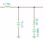
I have a low pass filter as below and I need to generate transfer function for this. (My ultimate goal is to plot frequency response of this circuit.)
How do I derive it?

I was thinking (Xr+Xc2)/Xr+Xc2+XL)...But what to do about Xc1?

Do I need to consider the RC branch for plotting the frequency response?
Snapshot.png

I will be using this circuit at the output of D amplifier. So does this RC in anyway has to do anything with speaker load?

Need Help! :|
Thank you.

Regards,
Archana.
 
Last edited:

I suppose, the input is at the most left and the output at the most right side - OK?
(Note, to avoid misunderstandings, always show input and output nodes.)
Of course, each branch must be considered.
The calculation of the transfer function is relatively simple.
* step 1: Calculate the equivalent impedance Z2 of the parallel braches.
* step 2: Write the voltage division rule for Z2 and sL1 (s is the complex frequency variable):
* step 2: Rearange the expression to get a polynominal (in "s") in the numerator as well as the denominator.
 
  • Like
Reactions: AJAB

    AJAB

    Points: 2
    Helpful Answer Positive Rating
ok. I followed below steps...
Xx = Xc1 || (Xc2+R)

Then Vout/Vin = Xx/(Xx+XL)
The Plot I get with this calculation does match with the simulated one.
Thank you.

And yes I will surely specify the I/O nodes next time. :)

Thanks LvW.
 

Hi,

I have one more query for this ckt, regarding the DC power dissipation in the inductor.
If V is the supply to the internal MOSFETS of Class D amplifier, F is the switching frequency of PWM output, and IndR is the DC resistance of Inductor.
Can I say, Current through Inductor IL = V/2*F*L
And Power Dissipation = IL * IndR

Is this approximation correct?

Thanks,
Archana.
 

Status
Not open for further replies.

Similar threads

Part and Inventory Search

Welcome to EDABoard.com

Sponsor

Back
Top