Continue to Site

Welcome to EDAboard.com

Welcome to our site! EDAboard.com is an international Electronics Discussion Forum focused on EDA software, circuits, schematics, books, theory, papers, asic, pld, 8051, DSP, Network, RF, Analog Design, PCB, Service Manuals... and a whole lot more! To participate you need to register. Registration is free. Click here to register now.

Timing constrain the ADC to FPGA data path

Status
Not open for further replies.

matrixofdynamism

Advanced Member level 2
Joined
Apr 17, 2011
Messages
593
Helped
24
Reputation
48
Reaction score
23
Trophy points
1,298
Activity points
7,681
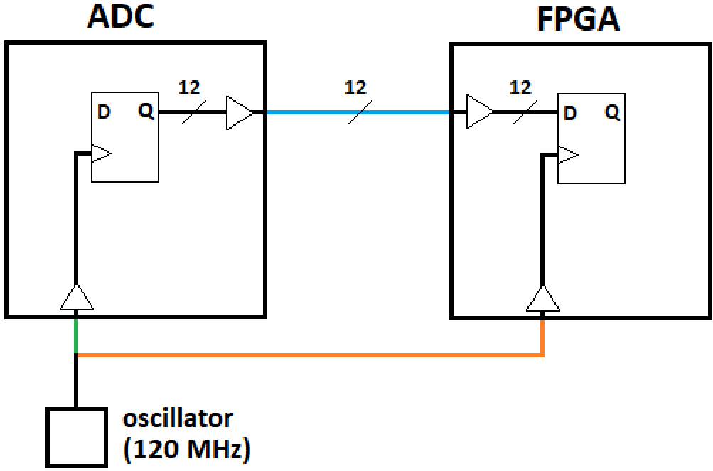
An ADC uses 12 single ended CMOS signals to transfer data to an FPGA. Both of them share 120 MHz source on the PCB. However, the PCB delay from the oscillator to the clock pin of each component is different. Here is the conceptual diagram where the PCB tracks are color coded. There are 12 PCB tracks for the data since the data is transferred parallely.

I have no clue how to constrain these 12 timing paths. They all involve delay on PCB tracks. How should the user constrain these paths using SDC commands? I think that I need to use some sort of add min delay, add max delay e.t.c in some way.
Untitled.png
 

@matrixofdynamism
You can use the SDC command as mentioned by Barry above.
Else you can also use Input Delay primitives inside the FPGA to align edges.
I prefer the SDC method as it is faster to implement.
 

Is there an application note that you know that describes how to constrain this? It is not just the delay in the data path signals. There is also the clock skew between the two clocks from the same source.
 

Is there an application note that you know that describes how to constrain this? It is not just the delay in the data path signals. There is also the clock skew between the two clocks from the same source.
You’re overthinking this. The only thing that matters is the delay from the clock edge to the data arrival.
 
Hi,
I agree with Barry.

I´m no expert in this - so please experts correct me if I´m wrong.

As far as I understand it: The constraint is common for all data lines. But for me it seems you want to do an individual constraint for each data line.
You rather add meanders on the PCB to meet the timing of the datalines.
And I recommend to treat the clock signal from routing and trace length equally than the data lines (unless there is a dedicated approach that contradicts this)
Now the ADC datasheet tells you how much delay you can expect from rising_clock to data_out.
If you treat signals and clock equally this gives the information for your FPGA timing constraint. Consider worst case.
You may expect a signal speed of about 150mm per nanosecond.
But if all signals are treated equally the absolute delay does not matter at all.

I recommend to use paper and pencil and draw a realistic timing diagram of your signals.
Then you add worst case timings. This shows you whether it´s better (what results in better margins) to use the rising or the falling edge to latch_in the signals at the FPGA.

//
Just a remark. Your sketch shows a 120MHz clock that directly clocks out 12 data lines. And you say these are single ended CMOS signals. This is quite a high data rate for single ended CMOS signals. Can you please confirm that I understood correctly.
//

****
If you need more detailed assistance then you need to give the timing of the ADC and the PCB layout. So we can do some realistic calculations and give recommendations.

Klaus
 

Status
Not open for further replies.

Part and Inventory Search

Welcome to EDABoard.com

Sponsor

Back
Top