Continue to Site

Welcome to EDAboard.com

Welcome to our site! EDAboard.com is an international Electronics Discussion Forum focused on EDA software, circuits, schematics, books, theory, papers, asic, pld, 8051, DSP, Network, RF, Analog Design, PCB, Service Manuals... and a whole lot more! To participate you need to register. Registration is free. Click here to register now.

[SOLVED] Timer 555 Astable Multivibrator

Status
Not open for further replies.

DasPreetam

Advanced Member level 4
Joined
Jan 5, 2014
Messages
100
Helped
2
Reputation
4
Reaction score
2
Trophy points
18
Activity points
755
I feel like a total noob in asking this question, but here it goes...

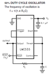
Wherever I read any article about the astable mode of timer 555, there is no clear explanation of the resistor R1 as shown in this figure...

I know that the capacitor charges through R1 and R2 and discharges only through R2. So, is it possible to omit R1 and charge capacitor through only R2 ?
 

The pin 7 end of R2 must have a positive voltage for the capacitor to be charged. But pin 7 does not produce a positive voltage because it is simply the collector of an NPN transistor that discharges the capacitor through R2 when it turns on and grounds pin 7. R1 provides the positive voltage at the pin 7 end of R2.

If R1 is simply a piece of wire then when pin 7 tries to go to ground the current from pin 7 will be very high and might burn out the 555 IC or burn out the power supply.
 
The function of R1 is described in many places. I added AN170 to EDABoard awhile back as it is no longer on NXP's site. Here's the link:


As Audioguru described, you need to consider the inner workings of the 555. This snippet illustrates AG's description. Note , R1 is labeled RA.

Capture1.PNG

On that same page of that application note, there is also a modified circuit in which the charge and discharge paths are separated by using diodes. That modification allows duty cycles less than 50%.

John
 

Okay thanks for the reply Audioguru... My doubts have been cleared. By the way, I've found another way of wiring the timer 555 in astable mode. It is given in https://www.robotroom.com/Infrared555.html site. It looks way unusual isn't it ?

On that same page of that application note, there is also a modified circuit in which the charge and discharge paths are separated by using diodes. That modification allows duty cycles less than 50%.
Yes, I knew that technique. Thanks anyways !!
 

Attachments

  • Cmos 555 oscillator.png
    Cmos 555 oscillator.png
    12.8 KB · Views: 76

So the charging and discharging path of the capacitor is same. Is this mode exclusively for the CMOS version ? Or can be used in NE555 also ?
 

An ordinary 555 can use the same circuit but since its output swing is not symmetrical (like the Cmos version) then the output is not truly square.
 

You can look at that circuit as simply a Schmitt trigger oscillator. The last page of Fairchild's AN118 on inverter oscillators describes that oscillator: https://www.fairchildsemi.com/an/AN/AN-118.pdf


Capture1.PNG


A pull-up resistor on the output may help with the non-CMOS 555, but I have not tried that.

John
 
Status
Not open for further replies.

Part and Inventory Search

Welcome to EDABoard.com

Sponsor

Back
Top