Continue to Site

Welcome to EDAboard.com

Welcome to our site! EDAboard.com is an international Electronics Discussion Forum focused on EDA software, circuits, schematics, books, theory, papers, asic, pld, 8051, DSP, Network, RF, Analog Design, PCB, Service Manuals... and a whole lot more! To participate you need to register. Registration is free. Click here to register now.

the size of NMOS trasistors of circuit

Status
Not open for further replies.

fati2014

Newbie level 2
Joined
Nov 10, 2014
Messages
2
Helped
0
Reputation
0
Reaction score
0
Trophy points
1
Activity points
17
hello,
I am beginner with CMOS transistors circuit. I am currently working on a project that is based on transistors.
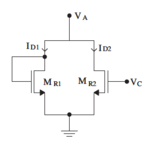
I'm working on sizing of NMOS transistors of attached file.
This circuit is an active resistance, but my problem is at the choice of parameters (W and L) of the circuit.
Can you help me to sized this circuit?
Kind regards. circuit_Mos.PNG
 

Hi
Can u tell us your spec? Look like missing some part of circuit?
 

Hi,
I am in the university and my specialty is electrical systems.
I do not know about that I forgot circuit parts because my goal is to have a circuit that simulate active resistance and I found this circuit in the literature. My problem now is how characterize this circuit and simulate it.
 

Hi
Just give 2 equals nmos minimum sizes (length, width) and assign Va a dc voltage. Sweep Vc from 0 to some dc number and plot Id1, Id2.
I expect Id1 is constant since it is in diode connection and Id2 will go from low to high current because you sweep its gate from 0 to some dc number
 

Can you elaborate on the purpose of VA? Is that voltage fixed by other circuitry?
 

Id1 is constant ( the MOS is in saturation because Vgs=Vds ) and Id2 is added to this current so R=Va/(Id1+Id2)
Id2 can be changed by Vgs voltage ( Vc ) and W/L ratio for M2 is easily found by applying inverse Id equation.There may be many W/L combination but starting with min. L will give you an aspect. Then you should consider max. allowable current per um^2 defined by your process and you play around w and L to get optimum solution.( Matching,Process sensitivity,noise,temp. effects etc)
 

This has lack of understanding written all over it.
Let the kid do his homework and read his book. This is a very simple circuit and a very simple concept.
the schematic is a simple exorcise to show the difference between active resistors and bias. ask yourself how do you set the currents Id1 and Id2...
hint: current is set directly by a current source in 1 and by ohms law in the other.
 

Status
Not open for further replies.

Part and Inventory Search

Welcome to EDABoard.com

Sponsor

Back
Top