pplus
Full Member level 4
In this case, you risk to overload the backup source. How do I know that produces 5V 300mA max standby 1.5 W, that is. But this solution can work.2-change in divider resistors network of tl431.
it cause 5vsb increase too. but 5v is useful for digital
3-adding some turns to 12v node in secondary of stand by transformer
I don't test it yet
some comments on your circuit:
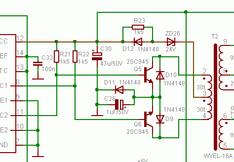
Microsim provide an additional source for TL494 buffer transformer. In your circuit voltage is limited by Zener diode ZD26, which works only when the spike exceed 24V relative to voltage on pin #12.
Last edited: