Continue to Site

Welcome to EDAboard.com

Welcome to our site! EDAboard.com is an international Electronics Discussion Forum focused on EDA software, circuits, schematics, books, theory, papers, asic, pld, 8051, DSP, Network, RF, Analog Design, PCB, Service Manuals... and a whole lot more! To participate you need to register. Registration is free. Click here to register now.

Switching of bridge FETs in an inverter

Status
Not open for further replies.

cupoftea

Advanced Member level 5
Joined
Jun 13, 2021
Messages
2,653
Helped
54
Reputation
108
Reaction score
116
Trophy points
63
Activity points
13,952
Hi,
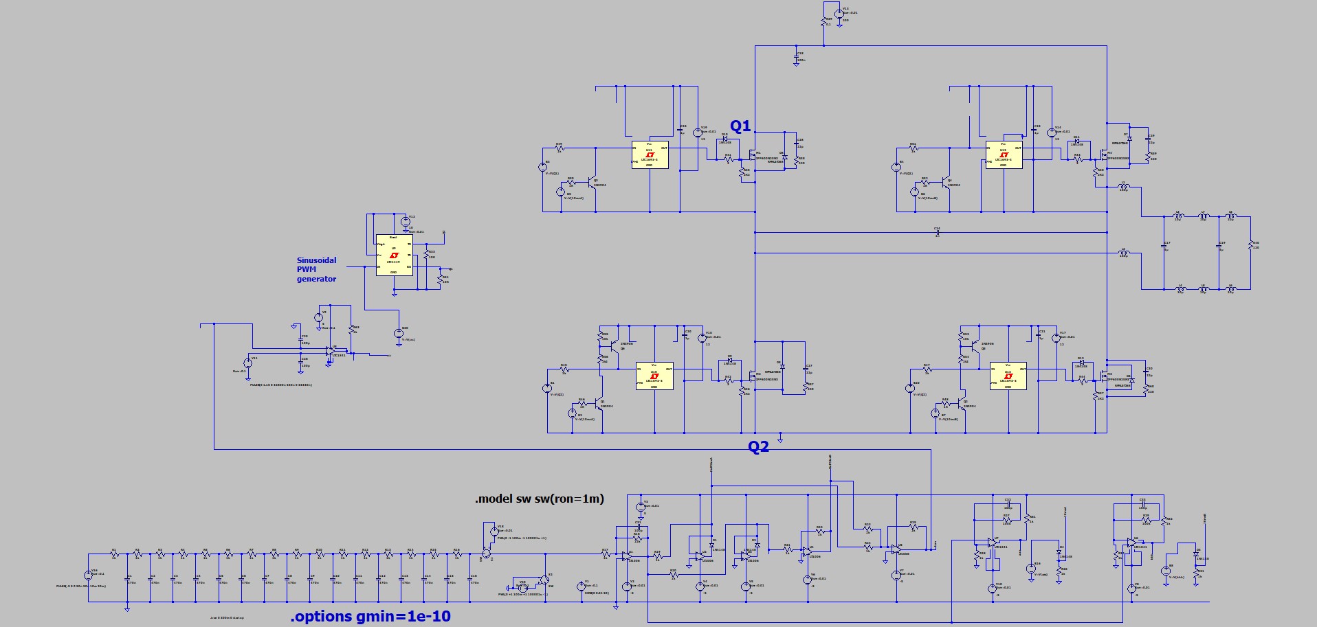
We are doing a non grid tied sinusoidal inverter.
VDC in = 190VDC, vac output = 110-126VAC.
As in the attached, the modus operandi is as follows...

1....For 10ms...Left leg FETs switch, and right leg top FET is OFF for the 10ms, and right leg bottom FET is ON for the 10ms
2....For 10ms...Right leg FETs switch, and Left leg top FET is OFF for the 10ms, and Left leg bottom FET is ON for the 10ms

....repeat above, etc etc

Is it possible to do a sinusoidal inverter, where the FETs switch together in diagonal pairs? (instead of same leg pairs)
Inverter simple.jpg
 

Attachments

  • 50hzINVERTER_jan3_SINE CHEAT.zip
    7 KB · Views: 120

Is it possible to do a sinusoidal inverter, where the FETs switch together in diagonal pairs? (instead of same leg pairs)
The schematic shows your old switching method, apparently. Why not sketch the intended switching pattern?
 
Thanks, actually, the attached sim in LTspice runs much quicker.
 

Attachments

  • Inverter_2_a.zip
    3.7 KB · Views: 85

Thanks, the question, was concerning, is the shown sims switching strategy, the only strategy used in doing inverters for mains (non GTI)?
Ie, switching the fets of one leg for 10ms, then the other leg for 10ms...etc etc
Or....
Is there a strategy involving switching diagonal fets for 10ms, then the other diagonal for 10ms, etc etc?
 

For " modified ' sine wave, the sw pattern is, diagonal pair on for 7.4mS, then bottom pair on, then other diagonal pair on for 7.4mS, then upper pair on - rinse and repeat.

for sine wave modulated pwm at higher freq, e.g. >= 20kHz, it is usual to have a fast leg with the SPWM and the other a slow leg switching at 100Hz - to provide the voltage inversion for alternate 1/2 cycles.

You can modulate both half bridge legs at the higher freq - but you simply incur more sw losses.
 
for sine wave modulated pwm at higher freq, e.g. >= 20kHz, it is usual to have a fast leg with the SPWM and the other a slow leg switching at 100Hz - to provide the voltage inversion for alternate 1/2 cycles.
Thanks very much, and i think from this, the "slow leg" has FETs held ON and OFF for 10ms at a time , so as such, it really needs a top side driver capable of holding the top fet on for 10ms ....so normal bootstrap drvers are not useable.....so therefore must use a hi side drive supply and eg a digital isolater to refer the gate signal up to the top fet's driver...would you agree?
 

Simulation showing current flowing up through either bottom mosfet while it's shut off, thanks to the body diode. (See Q3 Q4 scope traces.) The action is similar to a buck converter.

H-bridge switched at 60Hz. Notice upper Nmos, low-side Pmos.
Source is pulsed 190 VDC to keep it simple. Red wires are positive polarity.

H-bridge 4 mosfets (current flows upward) pulsed 190VDC becomes AC sine.png
 
Status
Not open for further replies.

Similar threads

Part and Inventory Search

Welcome to EDABoard.com

Sponsor

Back
Top