Continue to Site

Welcome to EDAboard.com

Welcome to our site! EDAboard.com is an international Electronics Discussion Forum focused on EDA software, circuits, schematics, books, theory, papers, asic, pld, 8051, DSP, Network, RF, Analog Design, PCB, Service Manuals... and a whole lot more! To participate you need to register. Registration is free. Click here to register now.

switch in charge pump in phase locked loop

Status
Not open for further replies.

Jalpa Pandya

Newbie level 5
Newbie level 5
Joined
Jan 20, 2014
Messages
10
Helped
0
Reputation
0
Reaction score
0
Trophy points
1
Visit site
Activity points
59
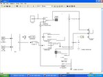
pll.JPG

in the above circuit there are NMOS and PMOS Current mirror circuits. PMOS SW and NMOS SW blocks represent the mos switches. the W/L ratio for Current mirror circuit is 10/0.18um. the W/L ratio for switches are 2.3/0.18.
If the w/l ratio is increased then the output current provided by the current mirror circuit increases and vice versa. Currently i am getting o/p current of 80ua for reference current of 100ua.
 

This occurs if you have different Vds voltages at your current mirror transistors, s. this image: Ids_vs_Vds.png . Just note the circles!
 

Take care (by design) that both mirror transistors have the same Vds. This is possible by control with an OpAmp.
 

Status
Not open for further replies.

Part and Inventory Search

Welcome to EDABoard.com

Sponsor

Back
Top