js0p
Junior Member level 1
substrate bias charge pump
Hello. I need to design a substrate charge pump to generate a negative substrate bias.
The picture shows a simple substrate pump basic cell proposed in the Baker Li "CMOS Circuit Design, Layout and Simulation".
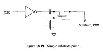
Can anyone tell me any formulas to design this circuit or where I can find those formulas?
For example, I wonder how can I calculate parameters like capacitor values, diode transistor sizing, oscillator frecuency, etc. for a substrate voltage, current and ripple required.
Thanks in advance.
Hello. I need to design a substrate charge pump to generate a negative substrate bias.
The picture shows a simple substrate pump basic cell proposed in the Baker Li "CMOS Circuit Design, Layout and Simulation".
Can anyone tell me any formulas to design this circuit or where I can find those formulas?
For example, I wonder how can I calculate parameters like capacitor values, diode transistor sizing, oscillator frecuency, etc. for a substrate voltage, current and ripple required.
Thanks in advance.