Continue to Site

Welcome to EDAboard.com

Welcome to our site! EDAboard.com is an international Electronics Discussion Forum focused on EDA software, circuits, schematics, books, theory, papers, asic, pld, 8051, DSP, Network, RF, Analog Design, PCB, Service Manuals... and a whole lot more! To participate you need to register. Registration is free. Click here to register now.

STM32 Interfacing with AD5940

uranyumx

Advanced Member level 4
Joined
Mar 5, 2011
Messages
102
Helped
1
Reputation
2
Reaction score
0
Trophy points
1,296
Activity points
2,093
Hello,

On my custom designed PCB, there is an AD5940 for impedance measurements with using the STM32F4 processor SPI communication.
My first target is that reading chip ID register to make sure that there is no issue between the processor and AD5940.
There are existing applications in github (https://github.com/analogdevicesinc/ad5940-examples) but when I download it,
I got an error message because I have a custom design board and they do with evaluation boards.
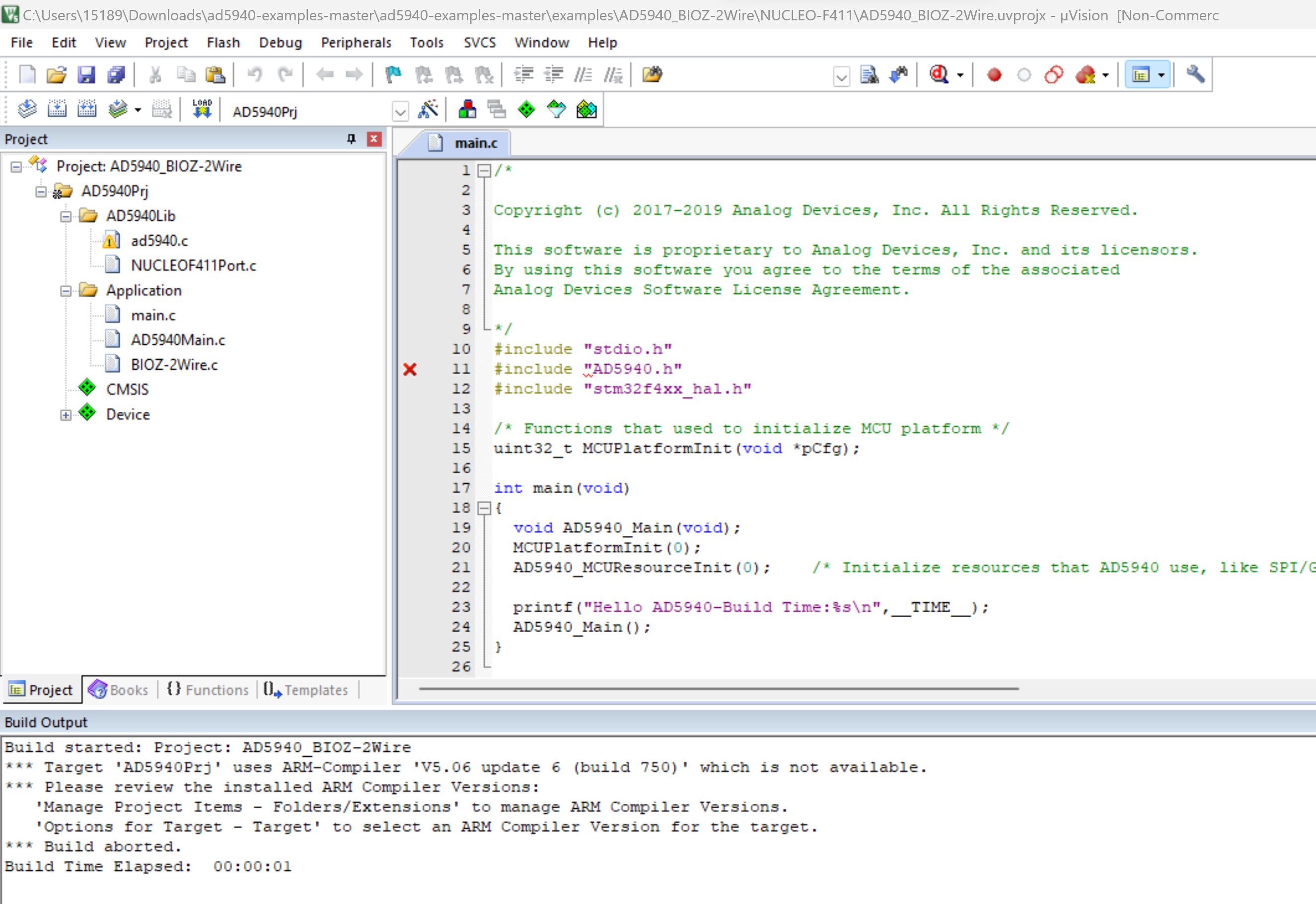
Keil Error.png
 
Now, I tested third step in the datasheet of AD5940, then I get this results:
Code:
...
int main(){

  uint8_t addr = 0x6D;
  uint8_t dummy = 0xCD;

  HAL_GPIO_WritePin(SPI3_CS_GPIO_Port, SPI3_CS_Pin, GPIO_PIN_RESET);
  HAL_SPI_Transmit(&hspi3, (uint8_t *)&addr, 1, 100);
  HAL_SPI_Transmit(&hspi3, (uint8_t *)&dummy, 1, 100);
  HAL_SPI_Receive(&hspi3, (uint8_t *)read_buf, 3, 100);
  HAL_GPIO_WritePin(SPI3_CS_GPIO_Port, SPI3_CS_Pin, GPIO_PIN_SET);
  ...

1687880180537.png
 
Hi,

My opinion:
Like already written in post#14 .... you show uncommented code
I wrote some lines of code for you including comments

Again, I don't spend tine on your posts to find
* what your code is supposed to do
* what and why you expect

You just keep your effort minimal and this makes it hard for us, time consuming, guessing ...
and in the end it makes it almost impossible for us to give focussed and good answers.

Klaus
 
Sorry for that, I updated the code with adding explanation. My target is that reading data from the register. Now I got certain values which were 0x1 in read_buf[0] but I am not sure whether this value is correct or not.

Code:
uint8_t addr = 0x6D; // Specifies read transaction. SPICMD_READREG
  uint8_t dummy = 0xCD; // A dummy byte

  // Read data from the register. Step 3 in page 99 of the AD5940 datasheet.
 
  HAL_GPIO_WritePin(SPI3_CS_GPIO_Port, SPI3_CS_Pin, GPIO_PIN_RESET); // Chip select pin set as low
  HAL_SPI_Transmit(&hspi3, (uint8_t *)&addr, 1, 100); // Send 8-bit command byte: SPICMD_READREG
  HAL_SPI_Transmit(&hspi3, (uint8_t *)&dummy, 1, 100); // Transmit a dummy byte on the SPI bus to initiate a read
  HAL_SPI_Receive(&hspi3, (uint8_t *)read_buf, 3, 100); // Read returning 3 bytes
  HAL_GPIO_WritePin(SPI3_CS_GPIO_Port, SPI3_CS_Pin, GPIO_PIN_SET); // Chip select pin set as high
 
Just going back to Post #20 - what address in the AD5941 are you trying to read?
By the look of your code it is 0xCDEF - and according to the data sheet no such register address exists. I *think* you are trying to read the chip identification register - according to Page 28 of the data sheet, the address for those are 0x0400 and 0x0404.
Trying to read from an invalid register address will probably be 'undefined'
Susan
 
Hi,

Thanks Susan.
@OP:
This is what I mean. We need to guess wgat you want to do, need to read your mind, need to read the datasheet, forward and back because your code does not match the datasheet. And so on.
We don't know what values in your read the registers you expect...

Klaus
 
Thank you @Aussie Susan and @KlausST

Here is my updated code to try reading CHIPID, but I am not sure that reading registers show correct result.

Code:
 write_buf[0] = SPICMD_READREG;
  write_buf[1] = 0x04; // myAddrH // Write CHIPID register
  write_buf[2] = 0x04; // myAddrL // Write CHIPID register

  // Read data from the register. Step 3 in page 99 of the AD5940 datasheet.

  HAL_GPIO_WritePin(SPI3_CS_GPIO_Port, SPI3_CS_Pin, GPIO_PIN_RESET);
  HAL_SPI_Transmit(&hspi3, (uint8_t *)write_buf, 3, 100);
  HAL_GPIO_WritePin(SPI3_CS_GPIO_Port, SPI3_CS_Pin, GPIO_PIN_SET);

  HAL_GPIO_WritePin(SPI3_CS_GPIO_Port, SPI3_CS_Pin, GPIO_PIN_RESET);
  HAL_SPI_Receive(&hspi3, (uint8_t *)read_buf, 3, 100);
  HAL_GPIO_WritePin(SPI3_CS_GPIO_Port, SPI3_CS_Pin, GPIO_PIN_SET);

1688075870556.png
 
Hi,

Please cooperate.
* document your code. Doing this you will recognize yourself that you don't keep on datasheet. I ask for this the third time now.
* instead of writing "I'm not sure ..." please write what values you expect
Please understand that both above is not for us only, it also is a simple tool to find mistakes on your own. Also to debug your code / maintain yozr cide even after years. If you don't cooperate, I will not cooperate either.

Datasheet says:
Writing to and reading from a register requires two SPI
transactions. The first transaction sets the register address(1). The
second transaction is the actual read (3) or write (2) to the required
register.
I just aded the numbers 1,2,3 here to clarify.
So the "two transactions" for
* a READ are: 1 + 3
* a WRITE are: 1 + 2

Also you are doing 3 bytes only in your "read function". I expect 4: command byte, dummy byte, 2 bytes register value

Klaus
 
I may be way off here but looking at the data sheet for the AD5940 and in particular the 'SPI Timing Diagram' (Figure 4, page 17), the STM32 SPI interface may be having a little trouble with this chip.
The issue is that you have set up the STM32 SPI interface correctly but the MCU will read data on the falling SCK edge. According to the AD5940 data sheet, the data on MISO will only be stable for a maximum of 27 nSec.
On some MCUs you can also specify (separately) when the MISO is sampled but I can't see that option on the STM32F4 (generic) data sheets.
What I'm thinking is that you may be sampling on the falling edge while the AD5940 is actually transitioning to the next bit value.
Perhaps something to check.....
Susan
 
Hi,

I agree, but first the OP needs to focus on the necessary code, steps by step
..... after this is done correctly then one can focus on timing.

Thus for future reference:
, the data on MISO will only be stable for a maximum of 27 nSec.
I don't think so.
T6 is the time from falling SCK to MISO stable.
During this time the MCU must not read the MISO value. It is unstable/delayed for 27ns. But after this time it's fine.
As raw estimationn this means that the SCK_LOW time must be >27ns (for 50% duty cycle: f_SCK < 18.5 MHz)
Datasheet says minimum 40ns LOW and 40ns HIGH and 62.5 ns period (how? While 40 + 40 = 80. Maybe 82.5ns?)

I'm rather concerned about the high delay of
* CS_LOW to MISO out (190ns)
* CS_HIGH time (80ns)
So depending on MCU speed it may be a good idea to put one or more NOPs after each change of CS.

The OP does CS_HIGH then immediately CS_LOW ... which may violate the 80ns spec

Klaus
 

LaTeX Commands Quick-Menu:

Similar threads

Part and Inventory Search

Welcome to EDABoard.com

Sponsor

Back
Top