Continue to Site

Welcome to EDAboard.com

Welcome to our site! EDAboard.com is an international Electronics Discussion Forum focused on EDA software, circuits, schematics, books, theory, papers, asic, pld, 8051, DSP, Network, RF, Analog Design, PCB, Service Manuals... and a whole lot more! To participate you need to register. Registration is free. Click here to register now.

Single Phase Half Bridge Inverter Design

Status
Not open for further replies.

Eshal

Advanced Member level 1
Joined
Aug 29, 2012
Messages
470
Helped
16
Reputation
32
Reaction score
15
Trophy points
1,298
Location
Nowhere :)
Activity points
5,149
Hello experts!

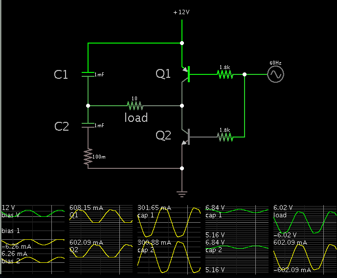
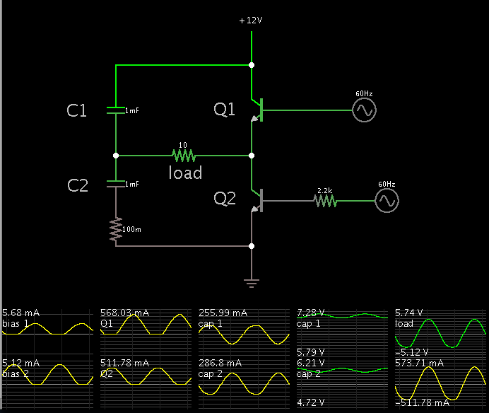
Here is the picture of Single phase half bridge inverter with R load only
single phase half bridge inverter.PNG
Here is waveforms with R load
waveforms with R load.PNG

My task is to design this inverter with proper values of C and proper Transistors, initially by choosing any Vs value and R value.

So, what if I start my designing by choosing Vs=12v? And if I choose R=10ohm.

I am not going to design it for any hi-fi values. Just small values of Vs and R. So what should be those values?

Thanks experts.
 

To choose capacitor values, use a similar approach as with a class A audio amplifier. The capacitor is in series with the speaker, to block the DC component, but pass AC.

The capacitor should be a high enough value that it passes the low frequencies.
The capacitor should charge to a stable DC level, not showing large voltage swings. Maybe 10 or 20 percent ripple.

My simulation shows 1000 uF is sufficient for both caps.

The transistors need to be rated for the entire supply voltage, and for the entire current you intend for the load to carry.
 

I think it is a guess that it should be around 1000uF. While I want proper calculation with assuming Vs and R values initially.
What did you choose Vs and R in your simulation?
Thank you sir.

Regards,
Princess
 

I think it is a guess that it should be around 1000uF. While I want proper calculation with assuming Vs and R values initially.
What did you choose Vs and R in your simulation?

I started with your values of 12V and 10 ohms.

For the bias, I started by applying DC pulses. The waveform through the load did not resemble a sine wave. So I changed the bias waveform to a sinewave.

I changed the high-side transistor to a PNP type, which simplifies matters so we can use a single control signal.

I watched the waveform through the load. I saw that small capacitors caused a distorted sinewave. I increased their values until I got a sinewave.

I continued to adjust values so that the load receives +6 and - 6 V amplitude. That is the greatest voltage swing I could achieve, with a 12V supply.

Screenshot:


To calculate the capacitor Farad value, I believe you would use the formula for capacitive reactance, at 60 Hz, with a series resistance of 10 ohms, plus whatever is the On-resistance of the transistor.

The formula is based on a single capacitor, because either of the capacitors can be omitted. Although they share the burden, only one is absolutely necessary.
 
  • Like
Reactions: Eshal

    Eshal

    Points: 2
    Helpful Answer Positive Rating
Thank you for your good reply sir
Please elaborate
I changed the high-side transistor to a PNP type, which simplifies matters so we can use a single control signal.
, why did you do so?
How it came in the mind that you should change high side NPN transistor to PNP?

The formula is based on a single capacitor, because either of the capacitors can be omitted. Although they share the burden, only one is absolutely necessary.
One capacitor? But we need Vs/2 across capacitor. So one capacitor can't do this job.
 

It should be mentioned, that the NPN/PNP circuit is good as a simple simulation setup, but not suitable for a real inverter design. Also driving BJT through a base resistor isn't a good idea because it involves huge power dissipation.

One capacitor? But we need Vs/2 across capacitor. So one capacitor can't do this job.
Vs/2 will be enforced by the average DC output of the half bridge, also for a single capacitor. The two capacitor circuit also includes the DC bus capacitor function and avoids transient currents on startup. In so far it might be preferred for a practical design.
 
  • Like
Reactions: Eshal

    Eshal

    Points: 2
    Helpful Answer Positive Rating
Thanks for your reply sir,
You mean if we are using BJT then we should not drive it through base resistor because it then dissipates power. Is it your mean?
And what should be suitable for real inverter design if not NPN/PNP?

One last thing, is it OK to use one capacitor as I got words from your script above. Can you please explain how one capacitor can perform job same as two capacitors, in easy wordings?

Thank you.
 

A real inverter would control both switches staggered with a deadtime between break and make, to avoid a bridge short or "shoot-through". This isn't possible with the simple PNP/NPN circuit. Furthermore you'll need to design a suitable control circuit for the utilized switch type and calculate the component values. My reservation is against the high base current and respective high resistor power dissipation with BJT switches, but it can be used. If you use e.g. darlington transistors, base current is low, but saturation voltage and switching losses are higher. I think that MOSFET switches are usually more convenient.

Regarding half bridge capacitors, if you assume a low impedance power supply or DC bus, bridge operation doesn't change if the capacitors are connected to ground or V+. So you can replace two capacitors with a single one of double capacitance.
 

How it came in the mind that you should change high side NPN transistor to PNP?

With 2 NPN's, we must create two different control signals, one inverted from the other.

Furthermore, the bias currents need to be tailored to provide undistorted sinewaves through the transistors.

My first simulation was with 2 NPN's (per your initial schematic). This is the best I could obtain.
The waveforms at the load are not as symmetrical nor as large amplitude, compared to my schematic in post #4.


I believe it is a good idea to test all possible arrangements of NPN and PNP.
Reasons:

There is the issue of creating a return path for bias currents. Notice that your upper NPN bias needs to pass through the load and a capacitor. If there is no definite path, the transistor will not turn on.

There is also the issue of shoot-through (per FvM's preceding post). It can waste a lot of power. Various methods should be tried, in order to reduce this.
 

@FvM
Good point. I was thinking of MOSFET too.
But I am still not clear regarding the use of one capacitor.
Here is operation of this single phase half bridge inverter, image attached.
Vs by 2.PNG and - Vs by 2.PNG
Here see, red lines shows the flow of current from Q1 to C2 and blue arrows show the flow of current from C1 to Q2.
Both transistors share both capacitor in their respective on time. So how could both transistors can share one capacitor for their operation?
If you can the kindly modify the schematic.
Thank you.

@BradtheRad
I am getting your point that why did you use PNP and NPN combination.
But I am unclear from this quote
With 2 NPN's, we must create two different control signals, one inverted from the other.
.
Because, NPN transistors are performing what we need i.e. Vs/2 and -Vs/2. Both are inverted.
And also, Both capacitors are needed, I think, because both are providing inverted Vs/2 voltages. How would one capacitor will do this job?

Thank you both of you.
 

Your assumption how current should flow through both capacitors is somehow arbitrary and contradicting physics in one detail: average of each capacitor's current over a total cycle must be zero. It's hardly possible that an unidirectional current flows through each capacitor during one halfcycle only.

While we can be sure that each capacitor's current has zero average, current sharing between both capacitors depends on the power supply impedance. For the ideal case of a pure voltage source, current is shared equally during both halfwaves. If you shift the V+ node of the upper capacitor to V-, capacitor currents will stay the same, but power supply current ripple increases.

As I already mentioned, the symmetrical capacitor topology is probably suggested for practical reasons, but not required in principle.
 
  • Like
Reactions: Eshal

    Eshal

    Points: 2
    Helpful Answer Positive Rating
But I am unclear from this quote

(BradtheRad): "With 2 NPN's, we must create two different control signals, one inverted from the other."
.
Because, NPN transistors are performing what we need i.e. Vs/2 and -Vs/2. Both are inverted.

A more common way to say it is that the two control signals need to be 180 degrees out of phase. This is shown in your timing diagram, post #1.

And also, Both capacitors are needed, I think, because both are providing inverted Vs/2 voltages. How would one capacitor will do this job?

This design can be looked at as a class AB amplifier. However you use a single supply. Therefore we borrow a technique commonly used in a class A audio amplifier, by using a single output capacitor to block DC. That way the speaker receives only AC.

Screenshot:


I was greatly helped by this article (at Rod Elliott's website). It goes into detail about the similarities and differences in the concepts of operation between class A and AB and B.

**broken link removed**
 
  • Like
Reactions: Eshal and FvM

    FvM

    Points: 2
    Helpful Answer Positive Rating

    Eshal

    Points: 2
    Helpful Answer Positive Rating
Nice answers from both of you. Great teaching. Thank you experts.
I will work on it further then let you know.

Thanks again.
 

Status
Not open for further replies.

Similar threads

Part and Inventory Search

Welcome to EDABoard.com

Sponsor

Back
Top