peanutnjelly
Newbie level 6

- Joined
- Oct 6, 2013
- Messages
- 11
- Helped
- 1
- Reputation
- 2
- Reaction score
- 1
- Trophy points
- 3
- Activity points
- 85
Hello everyone!
I am inexperienced in RF circuits, and I currently testing with some different circuits in "deadbug mode" to change that") .
.
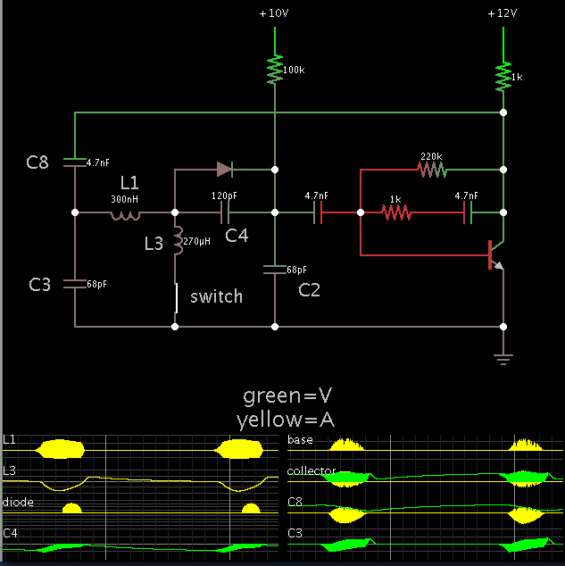
I am having a problem with this circuit:

All elements are the same except varactor diode is bb182.
Circuit is from Complete wireless design book.
Circuit starts to oscillate but it stops after about 4us and than starts again and again.

On left side of the board is almost the same circuit but without varactor(fixed frequency) and it works just fine at 50MHz.
On right side is mentioned circuit. For the time that it starts to oscillate frequency is 50MHz.

Any idea where is the problem?
I am inexperienced in RF circuits, and I currently testing with some different circuits in "deadbug mode" to change that
.I am having a problem with this circuit:
All elements are the same except varactor diode is bb182.
Circuit is from Complete wireless design book.
Circuit starts to oscillate but it stops after about 4us and than starts again and again.
On left side of the board is almost the same circuit but without varactor(fixed frequency) and it works just fine at 50MHz.
On right side is mentioned circuit. For the time that it starts to oscillate frequency is 50MHz.
Any idea where is the problem?