cupoftea
Advanced Member level 5
Hi,
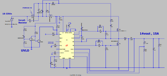
We all know the attached inrush limiting circuit, its well known, cheap-as-you-like, 2-penny-bit one that
uses the switching FET as a charge pump so as to provide the hi side supply for the Inrush-resistor-NFET.
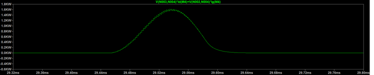
(LTspice and PNG attached, also inrush power waveform in the inrush NFET)
Crude, because the SMPS power current inevitably gets drawn through the just-turning-on inrush NFET.
Also, since the Vin range is from 18-33Vin, then you have to set the UVLO to around 16V, and then of course, if Vin
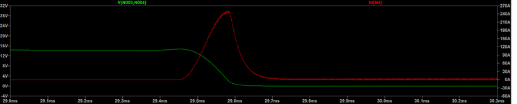
is 33V, then the inrush fet gets turned on prematurely and suffers an enormous inrush power spike which is
outside of its SOA. (as shown)
Adding a delay cap of some 10uF from D6 cathode to ground (as well as a diode across D15 to discharge it later)
appears to solve the issue, but has other problems.
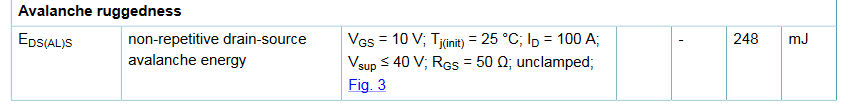
Would you agree that the attached inrush power pulse, would kill the PSMN1R8-40 NFET after about a year or so?
The VDS x IDS is within the SOA but after a year or so of this happening once per day?
PSMN1R8-40
We all know the attached inrush limiting circuit, its well known, cheap-as-you-like, 2-penny-bit one that
uses the switching FET as a charge pump so as to provide the hi side supply for the Inrush-resistor-NFET.
(LTspice and PNG attached, also inrush power waveform in the inrush NFET)
Crude, because the SMPS power current inevitably gets drawn through the just-turning-on inrush NFET.
Also, since the Vin range is from 18-33Vin, then you have to set the UVLO to around 16V, and then of course, if Vin
is 33V, then the inrush fet gets turned on prematurely and suffers an enormous inrush power spike which is
outside of its SOA. (as shown)
Adding a delay cap of some 10uF from D6 cathode to ground (as well as a diode across D15 to discharge it later)
appears to solve the issue, but has other problems.
Would you agree that the attached inrush power pulse, would kill the PSMN1R8-40 NFET after about a year or so?
The VDS x IDS is within the SOA but after a year or so of this happening once per day?
PSMN1R8-40
Attachments
Last edited: