Continue to Site
Follow along with the video below to see how to install our site as a web app on your home screen.
Note: This feature may not be available in some browsers.
TIP122 is on before TIP127 is completely off, the current through them can cause a lot of heat.
Put diode 1N4148 across R6 with cathode to the base of the transistor. Add 100pF from the base of the transistor to ground.
Do the same for R3.
For R1 and R9 the same but with the diode reversed (anode to base of transistor).
The idea is to delay the switch on of the power transistors, and not to delay the switch off. You may have to increase the 100pF if the problem is only reduced.
BTW, to my opinion the circuit isn't a clever design, if single transistors instead of darlingtons were used, and also PNP and NPN swapped the efficiency would have been the same but without the problem of both transistors conducting together.
You are right. I missed out important detail. You need also to change Q1-Q4 to 2N7000 (mosfet).Putting a diode 1N4148 across R6 with cathode to the base of the transistor, will it not bypass R6 in forward conduction. It would be that the ic is driving the transistor without any resistor. Placing a diode across R9 and R1, can the ic handle the discharge current of the capacitor?
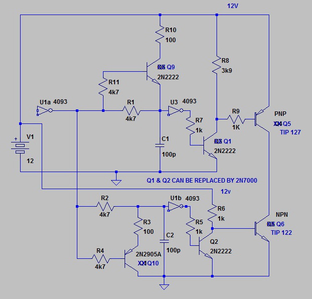
You are right. I missed out important detail. You need also to change Q1-Q4 to 2N7000 (mosfet).
- - - Updated - - -
will this modifications provide delay and avoid shoot through
Yes, it will avoid shoot through.
In your circuit Q1,Q2 don't need to be changed to 2N7000.
Vbase might need a simulator.
The usual faults are because Caps and Voltage sources in libraries have no ESR so infinite surge currents occur. I simply add where necessary the realistic values.I had a simulator once, it kept on finding faults
Q9 also present 100 ohms pull up
 affects Zout on emitter.