Continue to Site

Welcome to EDAboard.com

Welcome to our site! EDAboard.com is an international Electronics Discussion Forum focused on EDA software, circuits, schematics, books, theory, papers, asic, pld, 8051, DSP, Network, RF, Analog Design, PCB, Service Manuals... and a whole lot more! To participate you need to register. Registration is free. Click here to register now.

Seeking advice regarding structure of a DC-DC/PWM reg. for personal vaporizer.

Status
Not open for further replies.
Hi,

I thought you could calculate transition time by "t is the switching transient time (ton or toff)" (Zetex, DN80 "Bipolar transistors for MOSFET gate driving applications") - I'd understood you choose one or the other, I can't locate the second pdf where it also says the same/similar, along the lines of rise time + t on OR t off.

Probably "beginner WRONG assumption", but I'd assumed that if fSW is 0.00001s, then ton + toff would need to be below/within that 10uS, and the MOSFET would need to be turned on as "hard" as possible to avoid slowness and therefore also reduce switching losses, theory sounds so easy, practice probably not so.

Again, can't remember the web/document but it said, for what that may or may not be worth that gate current is - my apologies for such vagueness - (sic) "jaw-droppingly considerable in quantity" ...calculations I did shocked me, I must admit. Let's hope some-one who does this properly can answer more adequately.
 
  • Like
Reactions: David_

    David_

    Points: 2
    Helpful Answer Positive Rating
post #3 of this thread...
https://www.edaboard.com/threads/364892/

..tells you about switching loss calculation and drain voltage transition time etc.

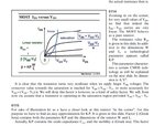
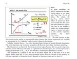
Basically you start getting switchign losses when charging ciss from vth to vgs(miller), and also when you charge cdg over its total voltage change in the switchign transition.

i = cdv/dt will calc your transition time.....and ohms law is what you use to calculate the Ig available to you
 
  • Like
Reactions: d123 and David_

    David_

    Points: 2
    Helpful Answer Positive Rating

    d123

    Points: 2
    Helpful Answer Positive Rating
d123, I have to admit that I lost track in checking out all the documents that you sent me. But I have put it up on my to-do list, as I only read 2-3 of them.

The document linked to in the post that treez referred to and lined to seems as a great resource, I have read up to page 10 and I will continue but I don't really get what I need and don't need or rather don't necessarily have to consider.
I have planned to write an Matlab GUI in which I(and others maybe) can input the datasheet parameters and get out the values one want to know, it is also in order to re-train my Matlab GUI familiarity, but first I have to re-read the document to understand what I need to know and not.

But my miss about "transition time"(which I noted the first time I dealt with those equations, but forgot about it...) means that my plan for how to build this thing has fumbled and I no longer have a solution for how to drive my MOSFETs. I can't yet be completely sure since I have yet to calculate the current that I am going to need as well as not definitely chosen a N-Channel MOSFET, the one I had thought to use would present(within the previous premiss) between 100 and 160nC gate-charge but I might need to look for one with a lower total gate-charge, the gate driver output voltage would have followed the battery voltage since I had planned to use a voltage doubler.

But one thing I'd like to ask that I simply can't figure out an answer for is this:

Is it possible to drive some logic-level MOSFETs with a voltage no higher than 3V?

I wonder because the lowest voltage I have at my disposal without any DC-DC converters is 3V and that rail can supply all the current I could ever need, but since it would appear that 3V is never enough to turn any MOSFET on ever I need to boost that voltage(which starts at 4,2V and ends up at 3V). I had planned to use a charge pump voltage doubler for this purpose but that only worked while I had made a large mistake while calculating(or estimating I don't know) the peak gate current.

Although I have been given the resources to calculate that(which I am in the process of understanding how to do) I reckon that since I previously had made provisions for switching the MOSFETs using about 20mA each(peak) under the assumption that the gates had 10µS to transition between states and that the total gate-charge was about 80-120nC. Then the new solution which might very well use MOSFETs with up to 160nC and not 10µS but perhaps a fraction of that the current requirements can probably not be satisfied by a voltage doubling circuit that can supply at maximum of 200mA.

I had really hopped to avoid using a second boost converter with inductor and all "only" to generate the gate driver supply voltage.

Granted this would all be very much easier if I where to choose to connect my batteries in series instead of in parallel but the point of this design has much to do with the possible output current which with series batteries would be limited to below 25A while the parallel configuration would allow for 50A(conservatively 40A)
so without doing this the hard way with parallel batteries it wouldn't really be any point in doing it at all.

Well sure it would but that 40A(50A) aspect is so important for me that it is parallel batteries that is going to be used.

As long as the circuit doesn't grow so large and complex that using 4 batteries as ether:
  • two series batteries paralleled with two other series batteries, or
  • two paralleled batteries in series with two other paralleled batteries, or
  • two series 26650 batteries(much larger but can output more current).
would make just as much sense, the thing is that since this in the very end would be a handheld device I obviously want it as small as possible.
But I have planned to build it with the batteries in the bottom of the device and the circuit on top of that since I wouldn't mind a longer device as long as it is small enough the be comfortable held with one hand. I haven't excluded the possibility that this might end up as a below the specs device but hopefully I can in the end of this hole thing be able to safely use it at 40A. I have probably written it already but I will be very thorough and careful when I get to testing this thing and there is no worry about that 40A capacity because it would not be used as such until I am sure about it all.
 

Earlier when I referred to a equation involving the total gate-charge and the transition time it came from the first page of this document.

I have yet to understand the implications of the document that treez linked to recently but nether am I done reading it, but I wonder about if the last equation of the above linked to document is valid?

Which is:
IG = QG/t(transition)
where:
IG is the gate current required to turn the MOSFET on in time period t(transition).
QG is the total gate charge.
t(transition) is the desired transition time.

In the document that treez linked to is says that practical switch on/off times of a power MOSFET is between 10-60nS, and since the procedure in that document seems very much more complicated than the equation above I just wonder if the following is really wrong some how.

My switching frequency is 100kHz and 60nS seems like a good enough ttransition time, I have found a MOSFET which at a VGS of 8V(which I have a boost circuit for generating) presents a total gate-charge of 45nC.

And since
45nC/60nS = 0,75A
then as long as I see to it that my gate drive can deliver ≦750mA(per MOSFET) and I include a gate resistor that would allow 750mA maximum, wouldn't I be OK?

I guess that this question is more about why that equation wouldn't be valid, is it valid and is the more involved way of deriving the gate current simply more precise so as to not over dimension the gate driver?
 

yes the document is this
https://reipooom.files.wordpress.com/2011/08/mosfet-must-read-2-slup169.pdf
..and its pages 4 to 10 that tell you how to get switching losses.

Your equation looks ok, but i wouldnt use it, because you have to go through the process to calculate t(transition).

Lets consider a CCM boost converter fet being switched on..
1)...first you charge cgs up to vth...this involves no switching loss in the fet
2)....then you have to charge cgs up from vth to vgs(miller)....while this i shappening, the FET current rises from zero to the peak inductor currrent level,
and the voltage across the fet is vout for this.....you calculate the time for this bit with i=cdv/dt.
vgs(miller) is calcualted using balogh's article page 5 at bottom
3)...then you have to discharge the cdg capacitor down to almost zero...again you use i=cdv/dt to get the time for this. forst calculate the energy for each
interval with V * I * t....but remember in the miller region, the voltage across the fet drops from vout to zero...so its (VOUT/2)*IOUT(PK) * t(discharge).

as discussed, its pages 4 to 10 you need to read....

Mind you, when you have say a CCM flyback and you want to do fet switch on loss, then its more complex because the leakage inductance mean that the current actually rises up from zero which reduces the switch on losses considerably.........thats why really you always need to do thermal testing and not realy on calculations on their own.
 
I see, or mostly. I can't even identify what it is but there is something that is really hard for me to grasp about this, but it is some fundamental thing that makes all my thoughts fussy.

I have read the document "Design And Application Guide For High Speed MOSFET Gate Drive Circuits" all the way through and have now gone back to pages 4 to 10 to write up all the equations and he main points of the explanation since it often helps to write it down even if you wouldn't use what you actually wrote. I don't believe I can have missed it so it appears that the equations contain variables not accounted for in the text, on page 4 is where equations first appear andthe first two is about the voltage dependence of CGD & CDS:
CGD ≈ CGD,0/(1+K1*√VDS)
CDS ≈ CDS,0/(K2*√VDS)

What is K1 & K2?
And what does the 0 refer to in CGD,0/CDS,0?

Do you know?

Then in the equation regarding the "Miller" effect it says:
CGD,eqv = (1 + gfs * RL) * CGD
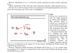
What is gfs?

One thing that makes this design easier is that the converters will never run continuously, not with any load to speak of anyway.
I haven't tackled the hole display stage yet(I need a small LCD or OLED, or something).

But imagining that I was using the device thought out in this thread right now, it would be used as I now will try to illustrate.

The time of activation(the time I hold down the "fire" button during which time the coils are supplied with power) will vary but they are always between 2-6 seconds normally, on occasion the time might be longer but the device will have a 10 second limit(which aren't being reached ever during normal usage and it is for preventing bad things happening from accidental activation). And during the most intensive usage the period between activation is about 5 seconds but such an intensive usage doesn't last for more than 3-4 activations all in all, at most. Most often there are anything between 30 seconds to several minutes or hours between activation, activation of 2-6 second duration.

I haven't yet decided about how long time there is going to be before the device enters into sleep mode but during the time it is not actively supplying the coils with power it shall operate in a power saving manner in which the load will be as good as non-existent compared to when it is supplying the coils with power.

I will think about thermal behaviour in any case, but the commercial devices I have looked inside use so small circuit boards that they simply have to rely upon the fact that the device is over all mostly in power save mode. One 200W devices PCB measures 80mm*16mm*1,6mm, and the PCB contains 6 MOSFETs out of 2 I don't yet know what they do but the other 4 MOSFETs are used for a synchronous buck converter(2 parallel for each switch).

And even though I can't tell how many layers it has nor how thick the copper is I still think that it is crazy small, isn't it?
Although the 200W isn't dissipated on the PCB but inside the atomizer containing the coils the power still travels pretty much over the hole length of the PCB from the battery connections to the atomizer connections.

My PCB will be a little* bigger than that, it might even end up as 2 separate PCBs.

I am almost starting to think that it might be better to use a higher number or larger batteries but in series in order to allow 40A while supplying between 6V and 8,4V since it would allow me to disregard the hole gate drive boost converter... Since it looks like that is going to dissipate at least something like 2W and I can't afford to use 2oz copper layers(the cost for 1oz is very much smaller).
And if I did that then all I would need is one single MOSFET in a buck converter, and that gate could be driven by the raw battery voltage. Besides the integrated buck converter for supplying the support circuits, I will have to think about the dimensions of such a design because it look a hole lot simpler.

The beauty of the two parallel18650 battery design is that the device was going to be small but this design is starting to look like it will take as much space as the 4 battery design which would have a lot simpler circuits. I guess it will all come down to how daring I will be with the space saving while counting on the short activity durations will mean the heat is no problem... Hm...
 

gfs is the mosfet's transconductance, (see page 5 of Balogh article) ill try and answer the rest later.

- - - Updated - - -

CGD ≈ CGD,0/(1+K1*√VDS)
CDS ≈ CDS,0/(K2*√VDS)

What is K1 & K2?
And what does the 0 refer to in CGD,0/CDS,0?

i dont know k1 and k2, (the mosfet manufacturer would have to tell you them) but it doesnt matter because i use the equation at the bottom right of page 4.

CGD,0 means the capacitance of cgd when at has zero volts across it.
 
  • Like
Reactions: David_

    David_

    Points: 2
    Helpful Answer Positive Rating
Hi,

Maybe that K refers to k/k' or Kn/Kp or this K with the formula on page 2.

This forum explains it quickly: k parameter in mosfet

The following slides are courtesy of: W. Sansen's Analog Design Essentials, chapter 1:

KP1.JPGKP2.JPGKP3.JPGKP4.JPGKP5.JPG

Not likely to be the K in the Wikipedia Current Source page, it's for Zeners and BJTs...
 
  • Like
Reactions: David_

    David_

    Points: 2
    Helpful Answer Positive Rating
I wonder about something, I don't know the math behind second-order filters but look at these pictures:
new_bbc_filter_wave.png
new_bbc_filter.png

First I had only one output inductor and three of the 47µF output capacitors, but then I split the value of that inductor(which will be made out of two equal inductors so it adds no extra anything) and placed 2 of those 3 capacitors after that inductor.

And look at the apparent results, the original output wave form looked like the "VOUT" wave form only about half as large in amplitude.

Is there any problems in these sort of configurations?

Is this really realistic? I wonder because using the same amount of L and C produces very different results, I have read regarding feedback loops that an second filter on the output can be problematic due to phase shift or something like that, but that was regarding analog PWM controllers. Do anyone know if the situation is different when using an digital software driven converter?
 

Hi,

Filter - active or passive - calculations seem quite hard. Sorry to ask, I'm not familiar with passive filters... Are you sure that's how to design a 2nd order (lowpass) LC filter? I don't know much, but it looks like a single LC stage after Vout :(.

I remember from one experiment a two-stage lowpass RC filter attenuated the original signal ("a lot") and was incompatible with the required amplitude... the maths looks horrid, but you should be able to bungle your way through it enough and gloss over the harder parts by resorting to trial and error simulations as filters affect phase, amplitude and ripple, allpass can be used to shift phase (back) to where it is supposed to be. Also, experiment, and all those diagrams of response based on Q and n^orders, etc. show that quite a few stages would be the desired for sharper response but space often makes that unlikely on a pcb.

Probably worth getting an overview of what filters do - TI, Analog Devices, a short National Semiconductor app note (search for IntroToFilters), loads of other resources show the salient points to expect to see with active (and some start with a description of passive) filters: gain, stages/Q, whether Butterworth, Bessel, Chebyshev, Demi Roussos or something would be more useful, I assume some is applicable to understanding passive filters.

It's better to do a bad and misunderstood calculation procedure first and continue from there than to throw components together as filters are yet another large world - tiny differences can have interesting effects. Look for a filter calculator online, maybe even Coilcraft or similar have such things.

I don't know if phase shift is a problem in your design, but the allpass can be used to correct that, as mentioned.
 
  • Like
Reactions: David_

    David_

    Points: 2
    Helpful Answer Positive Rating
Are you sure that's how to design a 2nd order (lowpass) LC filter? I don't know much, but it looks like a single LC stage after Vout :(

That sentence made me smile, because no I have no idea. I just tried something and it seemed to results in considerable effects.
I have read many documents about second order filters and nothing I have seen in those documents look like this. First of, the second inductor seems to always be very small in comparison to the first and the second capacitor is often recommended to be 10/1 the size of the first(if I haven't gotten those rations mixed up).

I actually started attending a mathematics class but my ADD/Aspberger got in the way because the school wasn't willing to lift a finger to resolve the mistakes that had been made while processing my application, I guess I will try it again because I need more math insights pronto.

Another issue that I experience is that documents often advertise as "here you will learn how to design *****" but then the document is obviously written for people whom already know what is going on within the subject of the document, that is at least how I experience it since I am getting no insights what so ever from them.

I have an important and critical design choice to make and then I can put together my first prototype, but the spice simulation of splitting up the filter components like that simply presented such a clean output that I have to consider it. But I have to choose one layout, Although since it is just a prototype I guess I can include footprints for both configurations.

Any way the critical design choice.

I have until now worked with the assumption that I will use 2*18650 batteries in parallel in order to realize 40A output current capability. But the circuit for doing that is starting to grow out of hand since I could opt for using 4*18650 batteries to realize 8,4V - 6V @ 40A. That would alter my device container design(which isn't done yet but I need to have a plan for it.).

The main points are that I can trade a doubling in the size the batteries take to gain:
  • No need for a separate boost converter since 6V is sufficient to drive the MOSFETs.
  • I can simplify the non-inv. buck-boost conv. into a simple buck converter(eliminating one of the diodes which will dissipate 18-22W or something around that). The maximum voltage output will be 5V so a buck is all I would need, possibly increasing the efficiency.
  • I can use a synchronous buck MOSFET driver to simplify the gate drive design while eliminating the other diode(another 18-22W save), all from choosing 1 IC.
  • My battery time would double(I think, or something close to that).
  • The over all system design would be much easier.
  • It would generally save me loads of time that I then could start putting into testing and software writing.

Actually looking at that list I feel compelled to go that way simply to get rid of those steaming diodes... 36W-44W isn't some minor heat dissipation...
My design for the container will be unlike anything ever seen on the market, I want a small device,but small in the sense that I can easily grab it with one hand and I wouldn't mind a slim shape that is weirdly long. Such as if I where to place the batteries in the bottom and then on top of that put the circuits which is the part of the device where the LCD would go and that my hand would grip around, I'll make an illustration tomorrow.

I actually got that synchronous buck MOSFET driver idea from working out how that Koopor Plus is built(talked about that early in this thread).
All such an IC requires in one single PWM input and the IC does the rest which is great.
 

So, I have decided to increase the number of batteries into 4 18650 Li-Ion batteries so that I get 8,4V - 6V while being able to draw 40A.

But another idea come to mind, since I now am going to use one of those nifty driver IC's often called something like "synchronous buck MOSFET drivers", it is an IC that accepts one PWM input and drivers both the high-side N-channel MOSFET and the low-side N-channel MOSFET replacing the diode in the non-synchronous buck converter.

But since the choice of inductor is still bothersome I was wondering if it couldn't be fairly simple to use two such "synchronous buck MOSFET drivers" in order to create two parallel synchronous buck-converters and then introduce a phase shift in the PWM signal in order to get a 2-phase synchronous buck-converter each of which delivers 20A when 40A are needed?

That would be great since there are more 20A inductors to choose from than there are 40A inductors to choose from.

Is there anything in particular I need to be aware of when driving buck-converters in parallel?
And what is the point of the phase shifting in the PWM signals?

There are a lot of info about multi-phase converters online but I haven't been able to find any really basic information.

- - - Updated - - -

No wait, forget those last questions.

I think I should stick with an ordinary synchronous buck-converter for now, since it is solvable I should do that first. I shouldn't take water over my head(or however that saying goes).
 
Last edited:

I think I have 3 things to adress:

1.
While reading about how to calculate the inductor value there are a almost standard to recommend the inductor ripple current to be set to 20%-30% of the maximum output current. And concidering a synchronous buck converter with a digital feedback loop, is there any point in keeping the inductor value "high enough" or is that 30% only to help determine the minimum inductor value so that you don't over dimension it?
In other words, is it possible to select a inductance that results in a too low inductor ripple current?

2.
I don't yet have a calculated value for the output capacitance (I have written up the equations though), but anyway. While looking at ceramic capacitors to buy (in this case 47uF, 100uF or 220uF rated at 6,3V or 10V) I found lots of them. But after having gone through the datasheet's for 7 different capacitors I couldn't find one single cap that in it''s datasheet displayed any information about the decrease of capacitance with applied DC voltage nor AC ripple voltage.
Temperature derating existed but not any other. And while researching how to design buck converters I came across examples telling and showing examples of such curves for the capacitors used.

How do I find capacitors with such ratings?

3.
I am confused about the design in some aspects, because while reading about how to determine components and all that I almost exclusively read about equations that tell me values.
But then on much less occurring instances I read texts talking about the components chosen but then in a frequency perspective relating to the control loop.
And I can't find any basic information about that at all and it seems to me as both perspectives should play a role from the beginning otherwise it seems as one are choosing components hoping that the feedback loop will work just fine and if it doesn't only then be concerned about that perspective.

Does any one have anything to say about this?

By the way, I really really appreciate all the help I have received. Thank you all very much.
 

2.
I don't yet have a calculated value for the output capacitance (I have written up the equations though), but anyway. While looking at ceramic capacitors to buy (in this case 47uF, 100uF or 220uF rated at 6,3V or 10V) I found lots of them. But after having gone through the datasheet's for 7 different capacitors I couldn't find one single cap that in it''s datasheet displayed any information about the decrease of capacitance with applied DC voltage nor AC ripple voltage.
Temperature derating existed but not any other. And while researching how to design buck converters I came across examples telling and showing examples of such curves for the capacitors used.

How do I find capacitors with such ratings?

Hi,

Murata ceramic GRM series show that info in the datasheets for the GRM range: e.g. page 13 Chip Monolithic Ceramic Capacitor for General GRM31CR60J107ME39_ (1206, X5R:EIA, 100uF, DC6.3V)

I think it was Murata who also had graphs of impedance Vs something or other, and other graphs, etc., but you'd have to dig into the website I can't find the link now, may have been AVX, presumably other manufacturers also will provide such information, but it may only appear in a catalogue, an app note, a page you'd need to search for a while on their site, etc.
 
  • Like
Reactions: David_

    David_

    Points: 2
    Helpful Answer Positive Rating
I don't yet have a calculated value for the output capacitance

Recently you had the idea of interleaving two or more buck converters. This brings an advantage because it produces waveforms which overlap and combine at the output, creating one comparatively smooth waveform.

Thus the output capacitor is not exposed to such severe current bursts as it is with a single converter. As a result you'll find you can get by with a smaller Farad value. In fact you may decide you can omit the output capacitor.
 
  • Like
Reactions: David_

    David_

    Points: 2
    Helpful Answer Positive Rating
I will look at those sites, in the case that I wouldn't find a capacitor that I can get my hands on that has any data I will just be conservative and assume a 50% de-rating(though for some reason I think it will be more something like 15%-30% using a 1210 package).

Yes I did consider interleaving at least two synchronous buck converters and I am still quit interested in that sort of thing but there are some rather big ? that I came to think was unnecessary to take on.

I don't know if I have talked about the inductor in this thread or in another thread but I thought I would need to use two 6uF coils in series to get 12uF with a high enough rated current.
But having done some more involved calculations I found that the minimum inductance is actually 1,8uH and choosing to use one of those two inductors,in other words using 6uH looks good.

As for the output capacitor, I don't see them as a problem since these day's it won't be especially expensive to buy capacitors that combine as a 500uF output ceramic cap(not de-rated).

But I don't know how the output capacitance effects the dynamics of the feedback loop.

But the main reason for why I abandoned the interleaved is that I don't know how the feedback will have to work.

First I need to use current-mode instead of voltage-mode, I hadn't decided upon voltage-mode yet but I feel unsure about how to manage the current sharing.

If I knew more about that then I would consider interleaving a couple of buck-converters.

The most recent development have been the discovery of the UCD7232 - Digital Control Compatible Synchronous-Buck Gate Driver with Current Sense and Fault Protection.

It looks quite cool,it provides the high-side and low-side gate drivers as well as the choice of controlling them both with 1 PWM signal or using 1 PWM for each of the MOSFETs.
Although I will only use the single PWM option, but besides that it also contains a high-gain precision switched capacitor differential amplifier and current limit comparator.
I haven't yet figured out all that I could do with it but the datasheet contains a procedure for calculating the resistor(s) and capacitor that are connected in parallel with the inductor and used to extract a waveform accurately representing the inductor current.
It's called something like zero DCR current sensing or something pointing to the fact that the inherent DCR of the inductor is used as the sense resistor.
It also have edge-blanking configurable with a resistor and a few other nifty functions.

Anyway I think it looks very promising for use in my project and since it makes the current sensing easy and the fact that I have access to the switched capacitor current sense amplifiers output I would think that this IC can be used for interleaved converters since I can combine the current sense signal of both ICs in a dual interleaved converter design.

But the fact remains that the only thing I really know about interleaving two converters is that I should shift the phase of one of the PWM signals with 180°.
I wouldn't think that I can't figure that out but I guess I am fearing that I would make it to hard for me to understand the feedback loop, but I don't know what my choice is going to be yet.

And if I go with the single simple synchronous buck converter I am really not far from assembling the first prototype and it is itching in my fingers by now.
 
Last edited:

Sometimes I feel that all the electronic related emails that I have signed up for mostly brings info about quite boring things, but from time to time I get gold nuggets in those mails(some types such as news from ADI, TI and LT are always interesting since the tell you about new high performance components, but I don't even know what "Testing Microwave Backhaul Radio Systems" is about...).

Anyway I found this through news emails: **broken link removed**
Which is a great walk through of how to select the inductor, input and output capacitor, freewheeling diode and then it ends up with some basic information about efficiency. The topology concerned is step-down fixed frequency PWM controlled converters operating in CCM mode("CCM mode", Continuous Conduction/Current Mode mode...). It is the best source for finding such equations I have come across.

In those articles they show this picture depicting the relationship between input capacitor ripple current vs VOUT/VIN which looks like this:


But I don't understand why the curve looks that way, I would have thought that the cure would increase in a linear fashion.
Do anyone know why the input capacitor ripple current starts out low when the ratio VOUT/VIN is low and then the input ripple increases as the VOUT/VIN increases and the input ripple maximum occurs when VOUT/VIN is equal to 0.5, but then the input ripple current starts to decrease with further increase of the VOUT/VIN ratio?

I have been trying to think about this but I can't come up with any answer at all and such a situation is always troublesome while one are designing a high current converter...
 

I would like to ask for advice to make up my mind about something.

I have made plans to use a UCD7232 to drive the MOSFETs of my synchronous buck converter and the circuit looks like this:
synch_buck_driver.png

Notice that the inductor current is sensed using it's DC resistance as the current sense resistor, UCD7232 contains as precision switched capacitor differential current sense amplifier who's output is put out on the IMON pin, at 0A the output voltage is 500mV and it goes up to a maximum of 3V.

But lately I have read some things that says that such current sensing isn't really good at all without temperature compensation in the microcontroller to account for the large temperature coefficient of the copper in the inductor. And I really don't need to add more things to be solved in the software, but I am still unsure.

A alternative would be to find another synchronous buck gate driver which contains simply the gate drivers and not all the fancy functions of the UCD7232 and then implement a current sense amplifier with sense resistor in series with the output inductor.

But also I will need to measure the resistance by some means that is put across the output, which is relevant since I need to know how much current is flowing through the output to be able to make sense of the voltage drop over that part of the circuit.

Do you know if there is a difference in the results gained from measuring the current directly across the inductor as opposed to measuring it in series with the output?


Given what I have told you, would you prefer one method before the other and if so why?

- - - Updated - - -

The UCD7232 also have a current limit set pin which could be driven by a DAC in my microcontroller to adjust the current limit at which value to gate drivers shut down,and it also have a resistor used to set the maximum voltage drop allowed over the high side MOSFET such that when that voltage is reached the gate drivers also shuts down, then there are also temperature protection and another type of protection that I can't recall what it was, when any of these failure modes are entered the FLT pin signals the microcontroller that something has happened.

So that high-side MOSFET voltage drop protection could be used to set a safety feature to never allow over ? Amps to flow and the adjustable(through the use of a DAC) current limit could be used to limit the current as a extra safety in case my control loop would fail which maybe it could considering that it is up to my coding to ensure safety...

So there are some nice features in the UCD7232, the question though is how viable that current sensing technique actually are...?
 

I gather that no one knows what to say about this, but I have found very different solution which I really like.

TI amongst others manufacture these integrated MOSFET drivers that also contain both MOSFETs for a synchronous buck-converter, I think I have decided to use CSD95472.

But it is weird, I will contact TI and ask them about it because I have never ever seen a TI part with a datasheet containing so little information. The only information you can find about the devices operation is the pin descriptions, which in this situation with a part like this may be enough but still it leaves many questions un-answered. A temperature compensated current sense circuit is included in the IC as well.

- - - Updated - - -

Oh, the CSD95472 have a maximum output current of 60A and the output is specified as 5.5V which I assume means that I can output voltages up to 5.5V with the current sensing and such functioning. Other companies similar circuits have a output voltage limit, sometimes that can be exceeded but then the current sensing circuit won't function. But TI's parts also have a reference voltage input used for the current sensing which I think can be used to tailor the range over which it will function besides the obvious use of matching that voltage to a ADCs input voltage.
 

Which information you are particularly missing in the CSD95472 datasheet.

TI apparently tries to establish an alternative to the DrMOS Integrated Power Stage standard issued by Intel, supported e.g. by Infineon, Fairchild, Vishay and others.
 

Status
Not open for further replies.

Similar threads

Part and Inventory Search

Welcome to EDABoard.com

Sponsor

Back
Top