Continue to Site

Welcome to EDAboard.com

Welcome to our site! EDAboard.com is an international Electronics Discussion Forum focused on EDA software, circuits, schematics, books, theory, papers, asic, pld, 8051, DSP, Network, RF, Analog Design, PCB, Service Manuals... and a whole lot more! To participate you need to register. Registration is free. Click here to register now.

S(1,1) and S(2,2) are positive while designing Power Amplifier MMIC

Status
Not open for further replies.

qasheef

Newbie
Joined
Jan 29, 2023
Messages
2
Helped
0
Reputation
0
Reaction score
0
Trophy points
1
Activity points
45
Hi
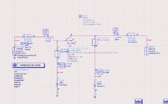
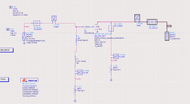
I am designing an X band amplifier using Win PDK MMIC kit.
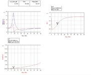
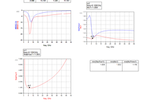
During initial analysis, with 50 ohm terminations at input and output port, the amplifier S(1,1) and S(2,2) are negative.
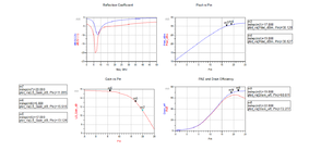
As a first step, i did load/ source pull using ADS built in template and get the Zs / Zl source and load impedances for max PAE. Then I inserted ZL as load impedance and conjugate of Zs as source impedance in ideal circuit, but the S(1,1) and S(2,2) becomes positive at frequencies from 1 to 8 GHz.

I have to add a resistor of around 24 ohm to make S(1,1) and S(2,2) lower than zero. But in this case, i am unable to get the performance from the transistor.

I am confused how to go about with the design. Should i first stablize the transistor and then go for design, for i should do the stability check at the end after making input / output matching network.
What can be the possible reason of having positive return loss in my design.
I tried to stabilize my transistor using a parallel RC network, however, the affect of Capacitance is negilible on the stability.
I am stuck how should i go forward with the design
 

Attachments

  • 11.jpg
    11.jpg
    193.7 KB · Views: 91
  • 12.jpg
    12.jpg
    119.3 KB · Views: 95
  • 13.jpg
    13.jpg
    183.2 KB · Views: 91

It's evident that your amplifier is unstable. Connecting a parallel resistor may also improve the stability. The first thing to do is to find the source of this instability. It's because output or input ?? You'd better check the Output and Input Stability circles first. If a parallel resistor is connected (200-300 something like that ) to Input or Output, the stability circles may be pushed out of the Smith Chart. There are also other techniques to improve the stability.
Small resistor (few Ohms) can also be added to Source or an amount of parallel feedback may also improve the stability. Operating Point is also Important.
Harmonic Termination is another key factor on stability..

Note : 50umx8 Periphery cannot give 30dBm Output Power @X band in my opinion. Check the dimension first to find the right specification.

Why Pin-3 and Pin-4 are not connected ??
 
Last edited:

Thanks Big Boss for the reply.
The 50x8 um device is GaN based device and generally gives the desired output.
Pin 3 and Pin4 are the thermal node pins and are required to be kept open if no external thermal circuit is being used.

For stability, i did the following steps,
I changed the bias point of Vg from -1.8 to -1.5 and did the load pull along with 10 ohm resistor. I got the the Z source and Z load values. Then I inserted a resistor in the gate bias line.
The major thing which makes the design stable is by changing the ideal inductor in the gate bias line with 0.1 nH inductor along with 40 ohm resistor in the line. The resistor in series at the gate is further down optimized to 5 ohm.

My device becomes unconditionally stable, with gain of around 12 dB and PAE of around 64 percent. However, i did HB analysis, my gain flatness is not that good actually. I want to operate my device around 19 dBm where i am getting maximum efficiency, however, the gain flatness is confusing me alot. Can you comment on it please.

I assume, once i start building the circuit, the issues of gain flateness will be solvled.

Since i need to use 4 transistors for power combining, so i think i just keep the 5 ohm resistor in series at the gate and leave the 40 ohm resistor at the gate bias line for introducing after the complete schematic design. is this approach feasible?
I am attaching design and displays for your kind comments.
 

Attachments

  • gain and P1db.png
    gain and P1db.png
    42.6 KB · Views: 78
  • ideal design layout.png
    ideal design layout.png
    52.1 KB · Views: 74
  • mufactor.png
    mufactor.png
    33.1 KB · Views: 80

LS_Gain_dB is not Gain Flatness, it's typical Gain Compression curve of an Amplifier. This is a normal behavior.
Sweep Pin from much lower value -for instance -40dBm- and take the Gain@-40dBm as a reference and check this Gain drops down to 1dB lower compare to Gain@-40dBm. This point will be your P1dB Compression point that is accepted as important PA metric for most of people.
Sweep Pin at the beginning coarse then squeeze the steps toward to P1dB Compression. In order to do that, use Sweep Plan
You should repeat Load Pull and Source Pull simulations because you have changed the circuit and something should have been changed. iteration is the key for RF design.

Pass through now to design Biasing Circuits. You will see that everything will be almost different.
This is a typical RF Design procedure. Step by step in a iteration.
 

Status
Not open for further replies.

Part and Inventory Search

Welcome to EDABoard.com

Sponsor

Back
Top