hot_snow
Junior Member level 1
Hello,
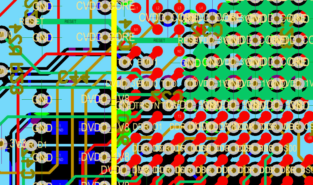
I have a 38mmx38mm PCB, my stack-up layer is like this: TOP/GND1/SIG1/SIG2/GND2/SIG3/PWR1/BOT.
I finished routing my board, now I try to make the partition of Power and GND. (It's the first time that I make a multilayer PCB)
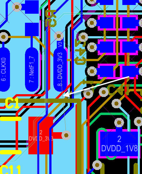
I have 2 GND planes connected to GND net and I have 1 power plane. I splited this power plane to 3 power levels (1.2v, 1.8v and 3.3v), also I used polygon pours in signal midlayers.
The problem is : When I run "the Design rule check", I have more than 500 rule violations. In fact, I have 2 types of rule vioalations:
Power Plane Connect Rule(Relief Connect )(Expansion=0.508mm) (Conductor Width=0.254mm) (Air Gap=0.254mm) (Entries=4) (All) 277
Un-Routed Net Constraint ( (All) ) 223
Well, All the rule violations are like this:
Starved Thermal on GND1: Via (27.06mm,24.55mm) Top to Bottom
.
.
.
Starved Thermal on GND1: Via (22.26mm,26.15mm) Top to Bottom
Starved Thermal on GND2: Via (27.06mm,24.55mm) Top to Bottom
.
.
.
Starved Thermal on GND2: Via (22.26mm,26.15mm) Top to Bottom
Starved Thermal on InternalPlane1: Via (19.06mm,26.15mm) Top to Bottom
.
.
.
Starved Thermal on InternalPlane1: Via (16.2mm,8.63mm) Top to Bottom
//////////////////////////////////////////////////////////////////
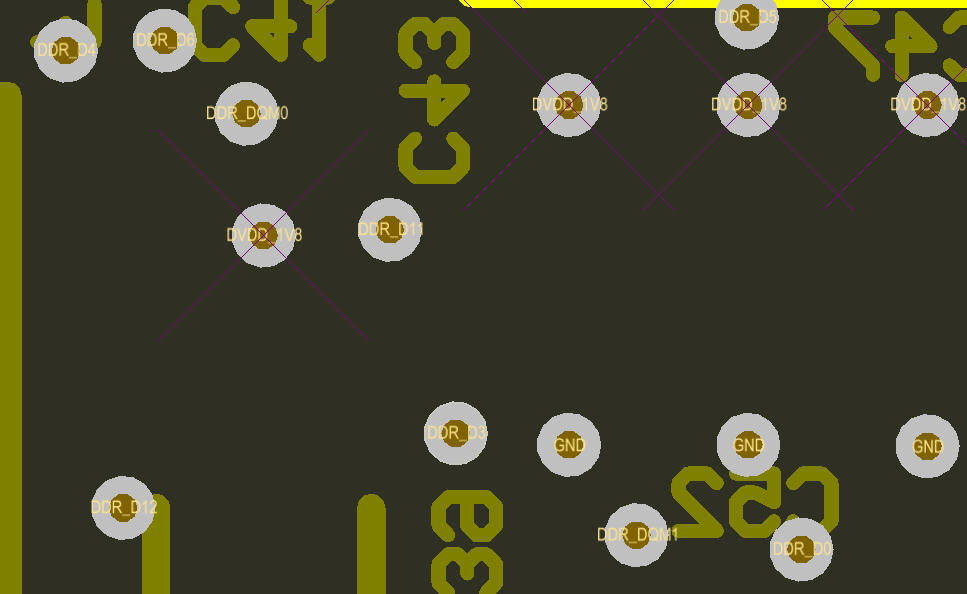
Isolated copper: Split Plane (GND) on GND1. Copper island connected to pads/vias detected. Copper area is : 8,4 sq. mm
.
.
.
Isolated copper: Split Plane (GND) on GND1. Copper island connected to pads/vias detected. Copper area is : 0,055 sq. mm
Isolated copper: Split Plane (GND) on GND2. Copper island connected to pads/vias detected. Copper area is : 8,4 sq. mm
.
.
.
Isolated copper: Split Plane (GND) on GND2. Copper island connected to pads/vias detected. Copper area is : 0,055 sq. mm
Isolated copper: Split Plane (CVDD_CORE) on InternalPlane1. Copper island connected to pads/vias detected. Copper area is : 16 sq. mm
.
.
Isolated copper: Split Plane (DVDD_3V3) on InternalPlane1. Copper island connected to pads/vias detected. Copper area is : 1,9 sq. mm
.
.
Isolated copper: Split Plane (DVDD_1V8) on InternalPlane1. Copper island connected to pads/vias detected. Copper area is : 0,52 sq. mm
.
.
What means all these errors?
Any help will be appreciated.
Regards,
I have a 38mmx38mm PCB, my stack-up layer is like this: TOP/GND1/SIG1/SIG2/GND2/SIG3/PWR1/BOT.
I finished routing my board, now I try to make the partition of Power and GND. (It's the first time that I make a multilayer PCB)
I have 2 GND planes connected to GND net and I have 1 power plane. I splited this power plane to 3 power levels (1.2v, 1.8v and 3.3v), also I used polygon pours in signal midlayers.
The problem is : When I run "the Design rule check", I have more than 500 rule violations. In fact, I have 2 types of rule vioalations:
Power Plane Connect Rule(Relief Connect )(Expansion=0.508mm) (Conductor Width=0.254mm) (Air Gap=0.254mm) (Entries=4) (All) 277
Un-Routed Net Constraint ( (All) ) 223
Well, All the rule violations are like this:
Starved Thermal on GND1: Via (27.06mm,24.55mm) Top to Bottom
.
.
.
Starved Thermal on GND1: Via (22.26mm,26.15mm) Top to Bottom
Starved Thermal on GND2: Via (27.06mm,24.55mm) Top to Bottom
.
.
.
Starved Thermal on GND2: Via (22.26mm,26.15mm) Top to Bottom
Starved Thermal on InternalPlane1: Via (19.06mm,26.15mm) Top to Bottom
.
.
.
Starved Thermal on InternalPlane1: Via (16.2mm,8.63mm) Top to Bottom
//////////////////////////////////////////////////////////////////
Isolated copper: Split Plane (GND) on GND1. Copper island connected to pads/vias detected. Copper area is : 8,4 sq. mm
.
.
.
Isolated copper: Split Plane (GND) on GND1. Copper island connected to pads/vias detected. Copper area is : 0,055 sq. mm
Isolated copper: Split Plane (GND) on GND2. Copper island connected to pads/vias detected. Copper area is : 8,4 sq. mm
.
.
.
Isolated copper: Split Plane (GND) on GND2. Copper island connected to pads/vias detected. Copper area is : 0,055 sq. mm
Isolated copper: Split Plane (CVDD_CORE) on InternalPlane1. Copper island connected to pads/vias detected. Copper area is : 16 sq. mm
.
.
Isolated copper: Split Plane (DVDD_3V3) on InternalPlane1. Copper island connected to pads/vias detected. Copper area is : 1,9 sq. mm
.
.
Isolated copper: Split Plane (DVDD_1V8) on InternalPlane1. Copper island connected to pads/vias detected. Copper area is : 0,52 sq. mm
.
.
What means all these errors?
Any help will be appreciated.
Regards,