Continue to Site

Welcome to EDAboard.com

Welcome to our site! EDAboard.com is an international Electronics Discussion Forum focused on EDA software, circuits, schematics, books, theory, papers, asic, pld, 8051, DSP, Network, RF, Analog Design, PCB, Service Manuals... and a whole lot more! To participate you need to register. Registration is free. Click here to register now.

Royer converter questions

Status
Not open for further replies.

narwhaler

Newbie level 6
Joined
Dec 7, 2012
Messages
12
Helped
0
Reputation
0
Reaction score
1
Trophy points
1,281
Activity points
1,426
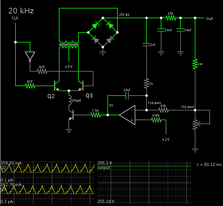
I've been looking for a very low noise (less than a mV p-p) medium voltage (~100 V) variable DC supply circuit for a photodiode power supply I'm building. I found the attached circuit in an application note from Linear Technology (AN-118). It is a resonant royer converter and the author claims 100 uV of noise at a 250 V DC output. The low noise is achieved through the resonant nature of the converter, which eliminates high frequency harmonics due to hard switching. I'm looking for some help understanding the circuit design and how I can modify it for my needs.

Royer.png

1. I assume the "x2" in the schematic by Q2 refers to the dual npn ZDT1048 (easy questions first :-D)

2. As drawn, the feedback to the negative pin of A1 does not equal the reference voltage at the positive input. If you have 250 VDC out, and divide that down by 500/1E6, that leaves 0.125 VDC at the negative input of A1. The positive input of A1 is tied to the internal 0.2V reference. Won't this drive the output way above 250V?

3. (Related to question 2) What is the purpose of the separate feedback paths (the 1meg/500ohm divider and the 0.001uF/1k path) - why would it be designed this way?

4. If I wanted to make this a programmable output circuit, could I just control the voltage on the + input of A1 from 0 to 0.2 V to swing the output from 0-250 V? If I wanted a different maximum voltage, could I just change the transformer T1 out for one with a smaller turns ratio (T1 Ns/Np = 67), and/or just change the feedback voltage divider? What I'm ultimately after is a supply that I can vary from ~20-100V.

5. Short of building and testing, how could I begin to analyze how this circuit will perform over temperature?

Thanks!
 

1. I assume the "x2" in the schematic by Q2 refers to the dual npn ZDT1048 (easy questions first :-D)

Makes sense. It implies the transistors are in a single IC, manufactured as a matched pair.

2. As drawn, the feedback to the negative pin of A1 does not equal the reference voltage at the positive input. If you have 250 VDC out, and divide that down by 500/1E6, that leaves 0.125 VDC at the negative input of A1. The positive input of A1 is tied to the internal 0.2V reference. Won't this drive the output way above 250V?

There are several components, each providing a certain amount of feedback. I believe the volt level at the inverting input varies above and below the 0.2V reference. As a result the op amp output adjusts to the net effect of the various feedback levels.

3. (Related to question 2) What is the purpose of the separate feedback paths (the 1meg/500ohm divider and the 0.001uF/1k path) - why would it be designed this way?

To reduce ripple perhaps?

There is a 430k resistor at the input. It reduces the effect of what comes from the resistor divider (namely DC), and emphasizes what comes through the .001 uF capacitor (namely AC).
 
2. As drawn, the feedback to the negative pin of A1 does not equal the reference voltage at the positive input. If you have 250 VDC out, and divide that down by 500/1E6, that leaves 0.125 VDC at the negative input of A1. The positive input of A1 is tied to the internal 0.2V reference. Won't this drive the output way above 250V?
Yes the component values don't make sense for 250V out. Seems like it must be an omission or error in the document.
3. (Related to question 2) What is the purpose of the separate feedback paths (the 1meg/500ohm divider and the 0.001uF/1k path) - why would it be designed this way?
The application note explains that it's a high frequency feedback path which provides improved transient response.
4. If I wanted to make this a programmable output circuit, could I just control the voltage on the + input of A1 from 0 to 0.2 V to swing the output from 0-250 V?
Yes, that would work fine.
If I wanted a different maximum voltage, could I just change the transformer T1 out for one with a smaller turns ratio (T1 Ns/Np = 67), and/or just change the feedback voltage divider? What I'm ultimately after is a supply that I can vary from ~20-100V.
Changing the turns ratio could work, if you're able to find a different transformer (might be difficult, unless you wind your own). Changing the bias voltage from 5V to something lower would probably work fine as well.

Good operation across a wide output voltage range might be tricky, since decreasing the output voltage inherently changing the drive voltage on the bases of the BJT. So at low voltages you may lose oscillation.
5. Short of building and testing, how could I begin to analyze how this circuit will perform over temperature?
The error amplifier should maintain DC regulation of the circuit regardless of temperature (except for maybe a bit of drift in the voltage reference). As for the output ripple and noise, that is harder to determine. The frequency of oscillation will likely change significantly, though the won't necessarily make noise worse. Increased leakage current in the rectifier diodes might also be an issue.
 
Thanks for the responses. Looking up the coiltronics transformer, they sell a similar model with a turns ratio of 50, so that drops me by a factor of 50/67 ~ 0.75. I'll have to work out what might be a lower limit for output voltage before base drive becomes an issue. The drive voltage on the base of the BJTs is set by the 820 ohm resistor connected to the supply voltage, so as collector drive current goes down the transistors will enter saturation, and at that point the circuit must stop oscillating as the additional base current does not drive the collectors any harder.
 

I'm looking for some help understanding the circuit design and how I can modify it for my needs.

5. Short of building and testing, how could I begin to analyze how this circuit will perform over temperature?

Thanks!

To better grasp how this circuit works, it helps to run it in an animated interactive simulator.

Screenshot (from Falstad's simulator):


It can export a link containing the entire schematic. If you click the link below, it will open the falstad.com/circuit website, load my schematic above, and run it on your computer. (Click Allow to load the Java applet.)

https://tinyurl.com/a5988u5

You can change values at will. Right-click a component and select Edit.

I changed a few things.

The simulator does not contain a transformer with three windings. So I substituted a pulse generator to drive the two transistors. I guessed at the frequency (20 kHz) and the primary Henry value (600mH). These seem to work okay.

I put a transistor on the op amp's output instead of a mosfet. The volt level was not high enough to sufficiently turn on the mosfet.

I made the capacitors smaller so the output will not take so much time to reach 250V.
I changed a 430k resistor to 43k.

I changed the 499 ohm resistor to a 1k potentiometer to see if it would provide variable output. However it appears that will require more effort to achieve.
 
BradtheRad - Thank you for the response. I'm intrigued to try your simulation but the link does not seem to be working properly. It takes me to the correct site, but then it just opens up an RLC circuit simulation. Can you double check the link?? Thanks!
 

Yes, the RLC circuit is the default.

I just clicked the link above. It still works.

I sometimes find that I must close all falstad.com windows and try again, if there was any glitch when opening his simulator page the first time, or if I visit later to import a second simulation.

You can also download his simulator package, free. It comes with a library of circuits. I will post the code for my circuit above, if you wish.

If you can get the website simulation to run, then you can export my circuit as text and paste it into a word processor for saving to disk.
 

Your posted circuit doesn't look to have much dead time for the push pull circuit, that is naturally provided by the Royer circuit, this may well give you hard switching and more "noise"than you are seeking...especially as you have removed the resonating cap across the transformer ends...
 

Status
Not open for further replies.

Similar threads

Part and Inventory Search

Welcome to EDABoard.com

Sponsor

Back
Top