Continue to Site

Welcome to EDAboard.com

Welcome to our site! EDAboard.com is an international Electronics Discussion Forum focused on EDA software, circuits, schematics, books, theory, papers, asic, pld, 8051, DSP, Network, RF, Analog Design, PCB, Service Manuals... and a whole lot more! To participate you need to register. Registration is free. Click here to register now.

ring oscillator frequency improvement by increasing the current

Status
Not open for further replies.

arya.jagadeesh

Member level 2
Member level 2
Joined
Jul 16, 2013
Messages
44
Helped
4
Reputation
8
Reaction score
4
Trophy points
8
Location
INDIA
Visit site
Activity points
285
in ring oscillator using cmos inverter if i wanted to increase the frequency.....i have to charge and discharge the capacitor faster ...so i wanted to increase the current ...by incresing width of transistor but this will work upto certain point......is there any other way to increase the current
 

Hi,
Techniques for increasing frequency are not a lot.
You can increase Vdd to increase your frequency. Another technique will require to select another kind of delay cell.
 

Look into layout geometry effects - for example, a FET
made of two stripes, center drain, will have less Cdb
than a single-stripe one of equal W. Similar Cgd though.
Which one dominates your shunt loading (bearing in mind
that Cgd is Miller-amplified)?

A lower-VT FET pair makes a hotter inverter (literally as
well). This is not often an option, but one I have made
some use of because I could.

You could consider moving to a CML type logic that will
run faster due to reduced voltage swing.

what are the frequency ranges that can be obtained by cml logic
 

You can design high speed circuit with CML but they will be power hungry. Frequency range depends on the technology that you will use.
 

CML will run octaves faster than bang-bang CMOS. Its tail
current is also a handy control-point (basically it's another
kind of current starved inverter, only it pulls current full time).

But when you're up against the inverter switching frequency
limit anyhow, there may not be much "cost" associated with
that DC bias - the inverters never settle to zero through-
current anyway, if you're not bottoming the square wave.

I've seen technologies that are capable of a couple of
hundred MHz in the standard cells (FF limited; inverters
can pass ~ 1GHz when appropriately scaled to the load)
make >5GHz prescalers using CML / SCL styles.

It's certainly worth a performance comparison. Bearing
in mind that you'll have further load current in the CML to
bang-bang level shifting.
 
Last edited:

my differential ring oscillator is not oscillating ....output is staying at constant dc voltage(output common mode).............what might be the problem....
 

Too perfect a DC solution will leave no error to "kick" the
oscillation. Perfect DC balance is a valid, though rare,
metastable state. Try adding a "kicker" current source
(like 0-1uA-0, 1nS rise/pw/fall) at the beginning of the
transient sim. Observing the circuit's startup / gain will
let you work on startup robustness.

first of all i thank you for your replies....
i have read that differential ring oscillator will work minimum 2 stages....
my design is working fine with 3 stages+output buffer ....if i am removing the buffer it is fixing at output common mode value...

in ade of cadence i am applying initial condition for one of input transistors by keeping 1....i think it is same as applying current source of short duration which you mentioned......

in designing i kept output and input common mode value at 1.6v based on conditions that i get to keep current sink in saturation.....that i got from minimum common mode level....for maximum common mode if i find i got condition that IR<Vt
of differential pair transistors ....

one more problem is that 3 stage+buffer is working for mos triode loads only ...if i am repeating the same thing with linear resistors it is not working....
 

Too little phase lag and too little gain sets you up for a
fail. More stages makes more gain. Many inverters have
poor gain at threshold, and worse elsewhere (I've seen
some with A=5, peak, DC). Removing the buffer is cutting
the loading and the phase lag on one of the stages.

You want bandwidth and gain in the individual stages,
but you also need 90 degrees of phase lag apiece in a
2-stage, 60 in a 3-stage, etc. - and if your gain has
dropped out by the frequency that gives you that
phase lag, you're hosed.

More stages, all of them faster, will be more robust
than a few slow stages. But I suppose the problem
is that your technology is marginal to the speed it
needs to produce.

In that case a single stage oscillator, followed by
gain (for digital swing) and buffering (for load), may
be your better option.
 

No. Saturation is where you get the most DC gain,
but this is not a DC gain problem - it's HF AC gain,
and you may need to push the transistors harder than
you would for a low power design. High-Z nodes, which
is what you want saturation-region operation for, are
going to be inherently low bandwidth. You want
bandwidth above all, in your situation, and that may
be a cascade of low gain high BW stages (gee, that
sounds sort of like a ring oscillator, now, doesn't it?).


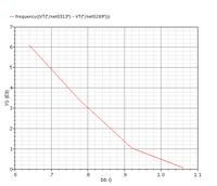
when i tried to tune the ringoscillator by varying the gate voltage applied to pmos load ...i got the graph as above ...bb is voltage applied at gate so actual vgs is vdd- bb.....in the above graph how to reduce the nonlinearity
 

i took more than 10 points in parametric simulation.........will increasing number of stages increase the linearity?
 

Status
Not open for further replies.

Part and Inventory Search

Welcome to EDABoard.com

Sponsor

Back
Top