Continue to Site

Welcome to EDAboard.com

Welcome to our site! EDAboard.com is an international Electronics Discussion Forum focused on EDA software, circuits, schematics, books, theory, papers, asic, pld, 8051, DSP, Network, RF, Analog Design, PCB, Service Manuals... and a whole lot more! To participate you need to register. Registration is free. Click here to register now.

[SOLVED] RF amplifier with one or two transistors

Status
Not open for further replies.

Nick_F

Member level 1
Member level 1
Joined
Apr 26, 2011
Messages
35
Helped
1
Reputation
2
Reaction score
1
Trophy points
1,288
Location
Sydney
Visit site
Activity points
1,614
Hi All,

I am looking for a circuit diagram of an amplifier with one or two transistors that can provide a gain of about 15dB to a level of 10dBm.
The operating frequency is 7MHz. Preferably, the transistors should be common types and the power supply 9 or 12V. Input and output impedance is 50 ohm.
I simulated some circuits in Spice, but they performed poorly when operating at such high levels.

Regards,
Nicolae
 

No simulation necessary. At 7 MHz, any 100 mW RF transistor (and most audio transistors) will work. The only thing to adjust is an optimum base bias and a tuned LC output circuit in the collector. And a good impedance transformer (tap on the output coil) to achieve a good power match to 50 Ohm load or antenna.You can check old radio-amateur circuit design for 7 MHz band.
 

Do you need it to work only at 7MHz?
Do you have a bandwidth requirement?
 

Do you need it to work only at 7MHz?
Do you have a bandwidth requirement?
A bandwidth of 1MHz would be good.

- - - Updated - - -

Do you want a linear amplifier?
Frank
Yes, it should be a linear amplifier receiving a sinewave signal and producing low distortion at the output.
 

No simulation necessary. At 7 MHz, any 100 mW RF transistor (and most audio transistors) will work. The only thing to adjust is an optimum base bias and a tuned LC output circuit in the collector. And a good impedance transformer (tap on the output coil) to achieve a good power match to 50 Ohm load or antenna.You can check old radio-amateur circuit design for 7 MHz band.
The purpose for this is for me to have a better understanding of RF circuits. I want to see what can be achieved with easy to find transistors. The simulation is very important to me. I expect to see a low amount of harmonics (> 40dB) and to use a pure 50 ohm resistor as a load and still have the 10dBm at the output.

I already built a few VFO's and the level after the JFET is very good (4Vpp - but on high impedance load). On one of the diagrams, there is a follower transistor (repeater on emitter) and next a standard RF amplifier but the level is too low. There is no tuning circuit in the collector. If I tried to increase the level, the distortion greatly increased.
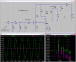
Based on your recommendation (and limited by my experience), I made the following circuit. At least in theory, it provides a good gain (30dB) and has an output level of about -3dBV ( = 10dBm).
I know there is some analysis to check if the circuit is stable. Maybe somebody can have a look and advise what improvements can be done. My main concerns is that I have no idea what the input impedance seen at the base of the transistor is and most likely there is a mismatch of impedances there (it can be seen there are pretty high distortion levels at the output of 3dB PI attenuator - which, I believe indicates a mismatch of impedances)
Many of the values of inductors, capacitors, resistors from the diagram are selected by successive tests, to see what gives the best results for simulation and probably they are far away from a perfect design.

Regards,
Nicolae

SH118.gif
 
Last edited:

The purpose for this is for me to have a better understanding of RF circuits. I want to see what can be achieved with easy to find transistors. The simulation is very important to me. I expect to see a low amount of harmonics (> 40dB) and to use a pure 50 ohm resistor as a load and still have the 10dBm at the output.

I already built a few VFO's and the level after the JFET is very good (4Vpp - but on high impedance load). On one of the diagrams, there is a follower transistor (repeater on emitter) and next a standard RF amplifier but the level is too low. There is no tuning circuit in the collector. If I tried to increase the level, the distortion greatly increased.
Based on your recommendation (and limited by my experience), I made the following circuit. At least in theory, it provides a good gain (30dB) and has an output level of about -3dBV ( = 10dBm).
I know there is some analysis to check if the circuit is stable. Maybe somebody can have a look and advise what improvements can be done. My main concerns is that I have no idea what the input impedance seen at the base of the transistor is and most likely there is a mismatch of impedances there (it can be seen there are pretty high distortion levels at the output of 3dB PI attenuator - which, I believe indicates a mismatch of impedances)
Many of the values of inductors, capacitors, resistors from the diagram are selected by successive tests, to see what gives the best results for simulation and probably they are far away from a perfect design.

Regards,
Nicolae

View attachment 83742

Your schematic looks good and may work well. I would use one-tenth of the base bias resistors values to make the amplifier more stable.
 

Thank you Jiripolivka. I will build this circuit (maybe in two weeks) and inform you about the results. I will lower the resistors as you advised.

Best regards,
Nicolae
 

Thank you Jiripolivka. I will build this circuit (maybe in two weeks) and inform you about the results. I will lower the resistors as you advised.

Best regards,
Nicolae

As you never mentioned the input power level, it may be useful to use a 10-kOhm potentiometer instead of the two base bias resistors, and adjust an optimum operating point for the transistor while monitoring the collector current with a mA meter. Please use an analog meter to see well the current change. Make sure the current does not exceed the maximum power dissipation of the transistor.

Good luck!
 

Your circuit show ideal conditions to be an oscillator around 7MHz as well. There is an old joke in RF design: To get an oscillator, try to build an amplifier. :wink:
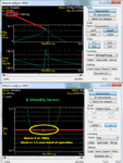
Look at the gain v phase of your circuit. You have massive gain (>40dB) around 8MHz, together with a rapid phase shift from -180° to 180°
Any stray capacitance or bad circuit layout may bump your circuit into oscillation.

The stability plot shows K going well below zero in your operating band. K should always stay above 1 with some margin.

Your design is unstable between 2-20MHz
 

Attachments

  • 7MHz_amp.gif
    7MHz_amp.gif
    105.3 KB · Views: 292
  • Like
Reactions: Nick_F

    Nick_F

    Points: 2
    Helpful Answer Positive Rating
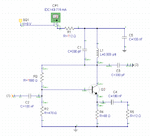
I'm tempted to be boring and just post up a classic circuit of a CATV based design using a 4:1 TLT and feedback to produce a broadband amp with very well controlled 50R input and output but here's a quick and dirty tuned version for 7MHz that should have +15dB gain and 50R input and output at 7MHz.

it should deliver +10dBm with low harmonic distortion.

The transistor will get quite warm and I'd recommend trying various types here to see how they affect linearity. eg 2N2222A, 2N3866 2N5109 2N3904 etc etc.

7mhz_amp.gif

- - - Updated - - -

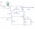
For completeness here's a quick CATV inspired design which gives about 15dB gain and should give a flat gain across a wide bandwidth (eg 1MHz to maybe 30MHz depending on the transformer design) It also should give good 50R input and output match across the entire frequency range because of the feedback techniques used.

This is based on a classic circuit and you can wind the 4:1 TLT on a FT37-43 ferrite core.


catv7.gif
 
Last edited:
I'm tempted to be boring and just post up a classic circuit of a CATV based design using a 4:1 TLT and feedback to produce a broadband amp with very well controlled 50R input and output but here's a quick and dirty tuned version for 7MHz that should have +15dB gain and 50R input and output at 7MHz.

it should deliver +10dBm with low harmonic distortion.

The transistor will get quite warm and I'd recommend trying various types here to see how they affect linearity. eg 2N2222A, 2N3866 2N5109 2N3904 etc etc.

View attachment 83879


- - - Updated - - -

For completeness here's a quick CATV inspired design which gives about 15dB gain and should give a flat gain across a wide bandwidth (eg 1MHz to maybe 30MHz depending on the transformer design) It also should give good 50R input and output match across the entire frequency range because of the feedback techniques used.

This is based on a classic circuit and you can wind the 4:1 TLT on a FT37-43 ferrite core.


View attachment 83880

i once saw a LNA with this kind of feedback to make a broadband before,and really interest in it,but i dont understand it well ,is there any pdf or book intruduce how this feedback work and how to design it? please help me
 

Simulation shows low level circuit oscillation (no input connected) at 6.8MHz as predicted by network analyzer results.
 

Attachments

  • 7MHz_amp1.gif
    7MHz_amp1.gif
    59 KB · Views: 206
Last edited:
  • Like
Reactions: Nick_F

    Nick_F

    Points: 2
    Helpful Answer Positive Rating
Try this:

amplifier.png

Voltage gain is -RL/R1 and if Rs=RL=R, output impedance = input impedance = Rf/(1-Av)
 

Your circuit show ideal conditions to be an oscillator around 7MHz as well. There is an old joke in RF design: To get an oscillator, try to build an amplifier. :wink:
Look at the gain v phase of your circuit. You have massive gain (>40dB) around 8MHz, together with a rapid phase shift from -180° to 180°
Any stray capacitance or bad circuit layout may bump your circuit into oscillation.

The stability plot shows K going well below zero in your operating band. K should always stay above 1 with some margin.

Your design is unstable between 2-20MHz
Hi,

Could you please tell me what simulation software did you use? Is there any software for stability analysis that is freeware?

Best regards,
Nicolae

- - - Updated - - -

I'm tempted to be boring and just post up a classic circuit of a CATV based design using a 4:1 TLT and feedback to produce a broadband amp with very well controlled 50R input and output but here's a quick and dirty tuned version for 7MHz that should have +15dB gain and 50R input and output at 7MHz.

it should deliver +10dBm with low harmonic distortion.

The transistor will get quite warm and I'd recommend trying various types here to see how they affect linearity. eg 2N2222A, 2N3866 2N5109 2N3904 etc etc.

View attachment 83879

- - - Updated - - -

For completeness here's a quick CATV inspired design which gives about 15dB gain and should give a flat gain across a wide bandwidth (eg 1MHz to maybe 30MHz depending on the transformer design) It also should give good 50R input and output match across the entire frequency range because of the feedback techniques used.

This is based on a classic circuit and you can wind the 4:1 TLT on a FT37-43 ferrite core.

View attachment 83880

Thank you very much for the schematics. The idle current is really high (40mA). I would be interested to see a gain and stability analysis of these amplifiers.

Regards,
Nicolae
 

Look around if you can find the free student version of Ansoft Designer. With this you could do stability analysis.

I used Multisim for the simulations. There is a free version but I am not sure if it includes all the instruments https://www.ni.com/multisim/
 
  • Like
Reactions: Nick_F

    Nick_F

    Points: 2
    Helpful Answer Positive Rating
Here's a screenshot of the CATV amplifier design.

You can see it has about 15dB gain across 2MHz to 30MHz and K>1 and B1>0 for stability.

You can also see it has good input and output match for a 50R system and should also produce +10dBm with harmonics much lower than -40dBc. But this is just a simulation.

It achieves the flat gain and the controlled I/O impedance through negative feedback. eg R5 lowers the gain as it get bigger but raises the input impedance as it gets bigger.
R3 lowers the input impedance as it gets smaller and also reduces gain through negative feedback. So if you get the balance of R3 and R5 correct you can get 15dB gain and also good device matching.

You should get good stability with this amp if you use a good PCB layout.


catv7_sim.gif

- - - Updated - - -

Here's a couple of simulations of lower current versions of the wideband and the tuned amp. You can see the harmonic distortion is higher but still (just) meets the -40dBc spec. However, this is just a simulation.

I would opt for a design based on the wideband version rather than the tuned one.

catv7a_sim.gif


eda7mhz.gif
 
  • Like
Reactions: Nick_F

    Nick_F

    Points: 2
    Helpful Answer Positive Rating
Thank you very much, G0HZU. I will build this amplifier as well and post the results.

Best regards,
Nicolae
 

Here's a screenshot of the CATV amplifier design.

You can see it has about 15dB gain across 2MHz to 30MHz and K>1 and B1>0 for stability.

You can also see it has good input and output match for a 50R system and should also produce +10dBm with harmonics much lower than -40dBc. But this is just a simulation.

It achieves the flat gain and the controlled I/O impedance through negative feedback. eg R5 lowers the gain as it get bigger but raises the input impedance as it gets bigger.
R3 lowers the input impedance as it gets smaller and also reduces gain through negative feedback. So if you get the balance of R3 and R5 correct you can get 15dB gain and also good device matching.
You should get good stability with this amp if you use a good PCB layout.
Hi G0HZU,
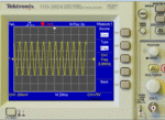
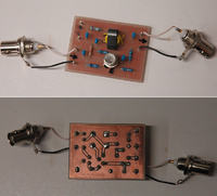
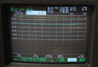
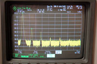
Your expectations based on simulation are very close to the real thing. I built the wideband amplifier and I will show in here the results. At 7MHz, the gain is about 16.9dB. I set the current to 30mA using R3 (increased from 330ohm to 1.2kohm). At 30mA, the second harmonics is -38dBc, while the output is set to 10dBm. If I increase the voltage, the current increases as well and I get over -40dBc for the second harmonics. At 50MHz, the gain is about 13.5dB when using a 2N3866. I also tried 2N3904 (tends to go into thermal runaway, second harmonics is -33dBc, gain is 16dB at 7MHz and 11dB at 50MHz). I also tried BC337 and it performs better than 2N3904 but not as good as 2N3866 (gain 16dB at 7MHz, 12dB at 50MHz, second harmonics -35.5dBc). By the way, I am not quite sure what does it mean a TLT 4:1. The transformer I built has 90uH on primary and 10uH on secondary (8 turns and 2 turns). Should the inductance be in ratio of 4:1 or the number of turns?

Best regards,
Nicolae

 
Last edited:

The 4:1 TLT is 4:1 impedance

Wind it as per fig 4C in the link below (i.e. the 4:1 transmission line transformer)

You have to be careful how you strap the two windings together and the image in the link below shows it quite well.

The 4Zo connection goes to the collector of the transistor.

The strap connection is the low impedance tap point and is the amplifier output.

The other connection should go to your RF decoupled supply voltage. This connection is shown as ground in the link below but you obviously need to connect this point to your RF decoupled supply in order to feed the DC to the transistor via the windings.

http://www.raylab.com/antenna/Transmission.htm

Yes, I would use a 2N3866 but you should really run a heatsink on it as it will run quite hot if you run it at high current.
 
  • Like
Reactions: Nick_F

    Nick_F

    Points: 2
    Helpful Answer Positive Rating
Status
Not open for further replies.

Part and Inventory Search

Welcome to EDABoard.com

Sponsor

Back
Top