chandra3789
Member level 1
hello frnds! plz help me out.....i am struck with a chronical doubt.....
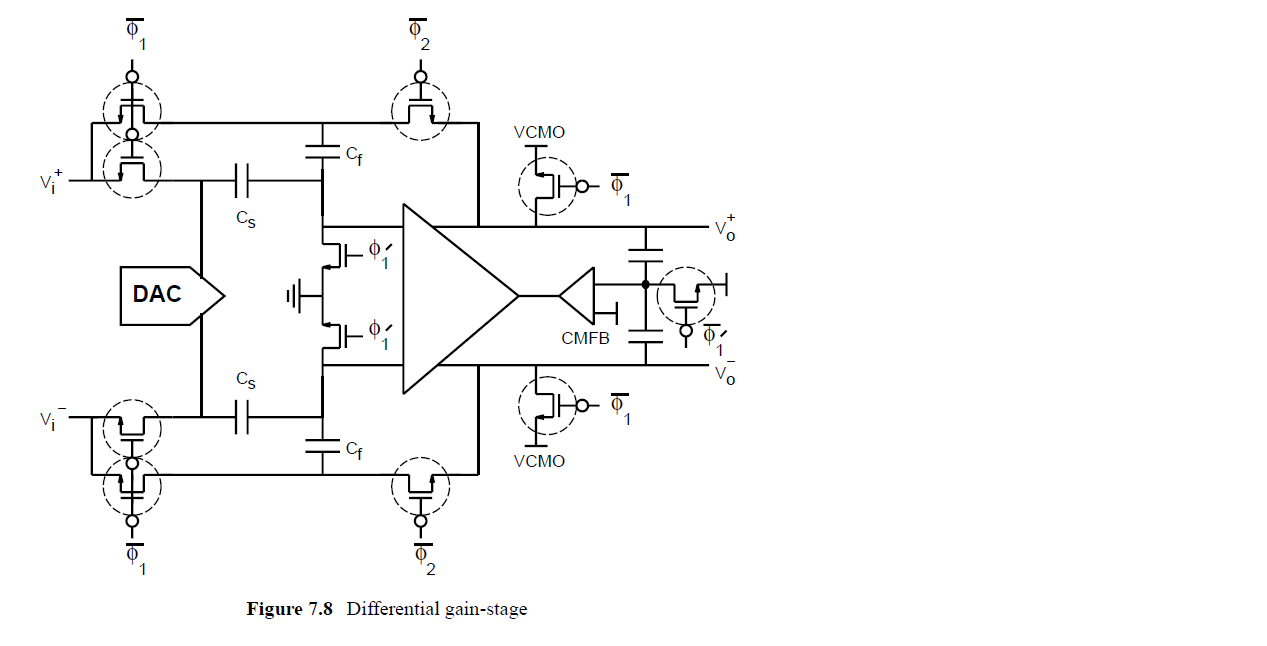
i am trying to simulate MDAC stage in 1.5 stage of pipelined ADC. The schematic i am using is shown in figure.
The designed op amp specs are
1.open loop DC gain = 68dB
2.UGB (1pF load) = 470MHZ
3. PM = 55 degree
4. Output swing = 0.35V to 1.35V with VOCM = 0.9V
5. ICMR = 0 to 1.1V with VICM = 0.5V
6.supply = 1.8V
I am applying common mode voltage at the node between the inputs of the op amp which is shown in the fig as ground.
now my questions are...
1.what should be the common mode voltage of the entire MDAC....is it 0.9V or 0.5V?
2. Should VICM and VOCM be equal?
3. The inputs should also have common mode voltage? or can i just give only signal there instead of common DC voltage?
4.If i use entire common mode voltage as 0.9V then if i want to apply 300mV step will it create a problem?(since 0.9V is at the edge of ICMR)
5. finally Gate boosted switches are really needed for sampling the input or just a transmission gate would suffice?
please reply to atleast some of the quesitons......if u see lack of clarity in my questions please let me know......