Continue to Site

Welcome to EDAboard.com

Welcome to our site! EDAboard.com is an international Electronics Discussion Forum focused on EDA software, circuits, schematics, books, theory, papers, asic, pld, 8051, DSP, Network, RF, Analog Design, PCB, Service Manuals... and a whole lot more! To participate you need to register. Registration is free. Click here to register now.

Reference plane for routing layer

engr_joni_ee

Advanced Member level 3
Joined
Nov 3, 2018
Messages
750
Helped
2
Reputation
4
Reaction score
4
Trophy points
18
Activity points
6,230
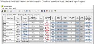
I just for a six layer stack up in Mentor Graphic tool were InterSignal1 (layer number 3) has a reference plane at layer VCC (layer number 2). Should not we always have GND at the reference plane ? For example InterSignal2 (layer number 4) has a reference plane at layer GND (layer number 5) which looks fine. The same reference plane at layer GND (layer number 5) can serve as reference ground for Bottom layer (layer number 6).

But how it goes with InterSignal1 (layer number 3) having a reference plane at layer VCC (layer number 2). Where will be the return path adjacent to signal layer which most text book says.
 

Attachments

  • Untitled 391.png
    Untitled 391.png
    190.9 KB · Views: 37
In a typical digital or mixed signal PCA, VCC will be bypassed to GND with 20 to 100 capacitors. Return path can be well shared by GND and VCC. In addition, return current is only relevant for single ended signals.
 
I am aware of the ceramic capacitors packages like 0603 as an example that we use between VCC and GND and we have these capacitors range from nF to some uF in order to remove ripples from power planes. But I think these capacitors are called de-coupling capacitors. What the difference between by-passing and de-coupling capacitors ?
 

LaTeX Commands Quick-Menu:

Part and Inventory Search

Welcome to EDABoard.com

Sponsor

Back
Top