Continue to Site

Welcome to EDAboard.com

Welcome to our site! EDAboard.com is an international Electronics Discussion Forum focused on EDA software, circuits, schematics, books, theory, papers, asic, pld, 8051, DSP, Network, RF, Analog Design, PCB, Service Manuals... and a whole lot more! To participate you need to register. Registration is free. Click here to register now.

RCD_snubber

Status
Not open for further replies.

Siddharth_saxena

Junior Member level 1
Joined
Nov 11, 2021
Messages
16
Helped
0
Reputation
0
Reaction score
0
Trophy points
1
Activity points
107
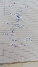
i have to figure out how voltage peak in switching depend on snubber capacitor , and snubber resistance . so i will take snubber circuit as a source-free parallel rlc circuit but according to my calculation zeta = (L/C)^1/2*1/2Rs
according to that Zeta is inversely proportional to c and rs. But logically as Rs and Cs increase the voltage peak will decrease ?
ase
 

Hi,

R = Resistor
C = capacitor
D = diode

I miss where in your formula the L comes from.

So either it´s the wrong formula, or there is an L we don´t know about.
Please clarify.

Usually it depends on the whole circuit (with swithcing circuit, any stray inductances, maybe load inductance)
Due to the diode the snubber s not active at the edge when the switch goes to ON state.
It also is not active during steady ON state
It will be active with the OFF edge ... and the following time.

Usually the peak current should be determined by the switch current at the time when the switch opens.

Klaus
 

voltage peak is come during switching but how it depend on snubber capacitance and resistance . Sir check the photo that i attached hope it is visible .
 

Attachments

  • WhatsApp Image 2021-11-23 at 15.38.24.jpeg
    WhatsApp Image 2021-11-23 at 15.38.24.jpeg
    81.5 KB · Views: 101

Hi,

now I see no "D" = diode.

Please clarify.
Your text needs to match with the schematic, otherwise it just results in confusion.

Klaus
 

okay , so can you help me to find out , how switching voltage peak depend on snubber capacitance and snubber resistance.
 

Hi,

without details i´s hard..

I´d go with the stored energy:
The energy in an inductance is: 0.5 x I x I x L
the energy of a capacitor is 0.5 x V x V x C

In worst case all the inductance energy is pushed into the capacitor.

Klaus
 

The RCD snubber acts like a buck-boost converter across the transformer primary.

1) It must absorb an inductive spike from the winding at Turn-Off.

2) This quickly charges the capacitor.

3) It discharges through the resistor during Off time.

Select RC values which result in minimum wasted Watts, and place minimum stress on R & C.
 

but how you can prove it mathematically that resistance and capacitance will reduce the peak of switching voltage ?
--- Updated ---

Hi,

without details i´s hard..

I´d go with the stored energy:
The energy in an inductance is: 0.5 x I x I x L
the energy of a capacitor is 0.5 x V x V x C

In worst case all the inductance energy is pushed into the capacitor.

Klaus
Hi,
so according to you 1/2 L*i*i=1/2C*V*V= constant so when C increases switching voltage is decreases?
 

hi,
my question what will be the effect of snubber resistance and capacitance on the switching waveform ? and if the voltage peak will decrease then how we can prove it mathematically ?
 

Attachments

  • 1637745150211.png
    1637745150211.png
    122.2 KB · Views: 87

Hi,

Isn´t it already explained?
What does your simulation show?

Mathematical formulas are given already.

Klaus
 

There's a formula telling what is the resulting voltage on a capacitor after a brief current surge goes through it.

Small C value, high voltage.
Large C value, lesser voltage.

The phenomenon of an Inductor producing a high voltage spike is one of those hard-to-explain curiosities of electricity. And it's fortunate that we can put it to practical use.

The resistor discharges the capacitor during idle period. The discharge curve is a familiar shape, the result of the RC time constant (R x C).
 
but how you can prove it mathematically that resistance and capacitance will reduce the peak of switching voltage ?
I presume you know that the differential equations discussed in post #3 don't describe a RCD snubber correctly, because they ignore diode operation.

Although not clearly stated in any of your post, you seem to design a fly-back converter (according to Multisim circuit title). Do you understand that you only need to absorb the energy stored in transformer leakage inductance? Your schematic however neither shows magnetizing nor leakage inductance. You need to specify it, as well as designed primary peak current to calculate snubber parameters.
 

Snubber design requires two quite separate steps.

First you need to know the energy that this snubber has to absorb. That will involve the energy released by an inductance "somewhere" when the current through it abruptly ceases.

The inductance may be difficult to define because it could be a real inductance, leakage inductance, or just parasitic inductance from physical wiring. Or a combination of all three. So maybe you guess, and assume energy released is a half LI squared.

That energy is dumped across a capacitor, which causes the voltage across the capacitor to rise. Again, if you know the energy, the change in voltage can be easily calculated.

Second step is to design a discharge circuit for our capacitor so it can recover fully before the next "event".

The frequency and duty cycle of our circuit tells us how much time we have to do the capacitor discharge.
There will always a diode associated with this, but basically the resistor will be sized to dissipate the required energy in the required time without unnecessarily high current.

As you have told us nothing about inductance, frequency, current ot time, its not really possible to come up with any realistic values without that information.
 

Status
Not open for further replies.

Part and Inventory Search

Welcome to EDABoard.com

Sponsor

Back
Top