Continue to Site

Welcome to EDAboard.com

Welcome to our site! EDAboard.com is an international Electronics Discussion Forum focused on EDA software, circuits, schematics, books, theory, papers, asic, pld, 8051, DSP, Network, RF, Analog Design, PCB, Service Manuals... and a whole lot more! To participate you need to register. Registration is free. Click here to register now.

RC oscillator design cadence

Status
Not open for further replies.

kenambo

Full Member level 6
Joined
Feb 26, 2012
Messages
393
Helped
52
Reputation
104
Reaction score
48
Trophy points
1,308
Location
India
Activity points
3,859
Hi all

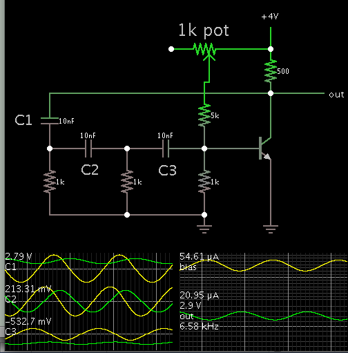
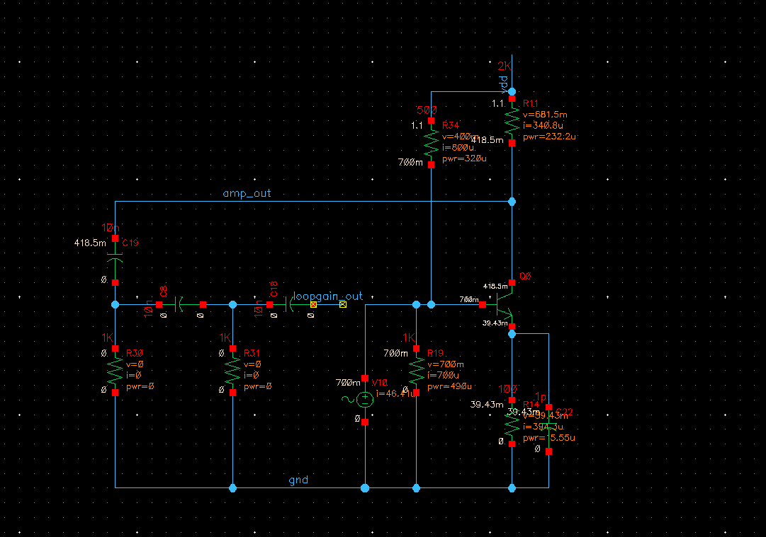
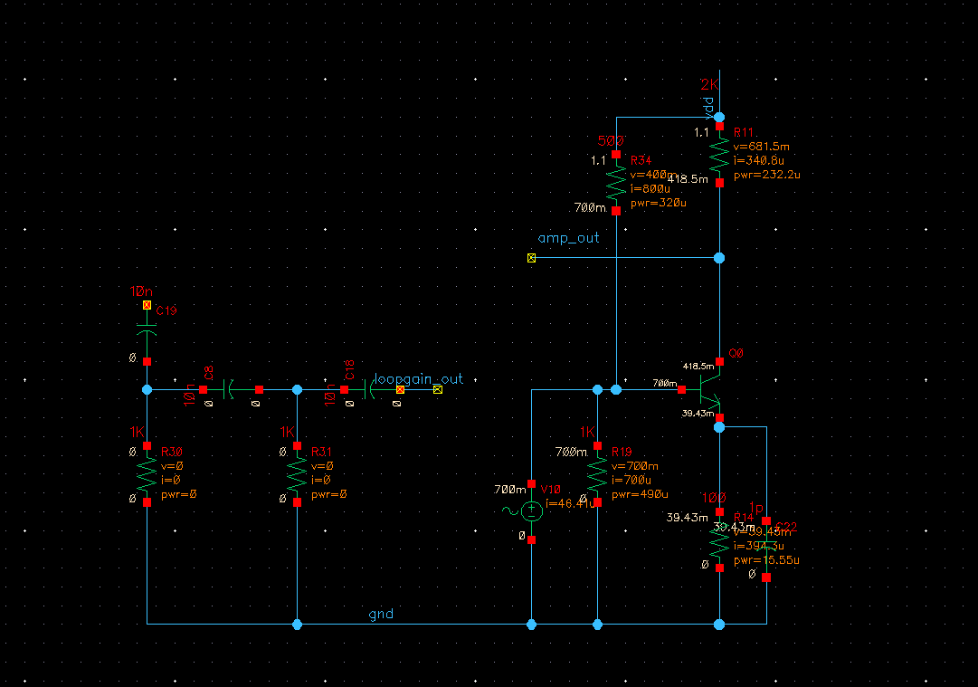
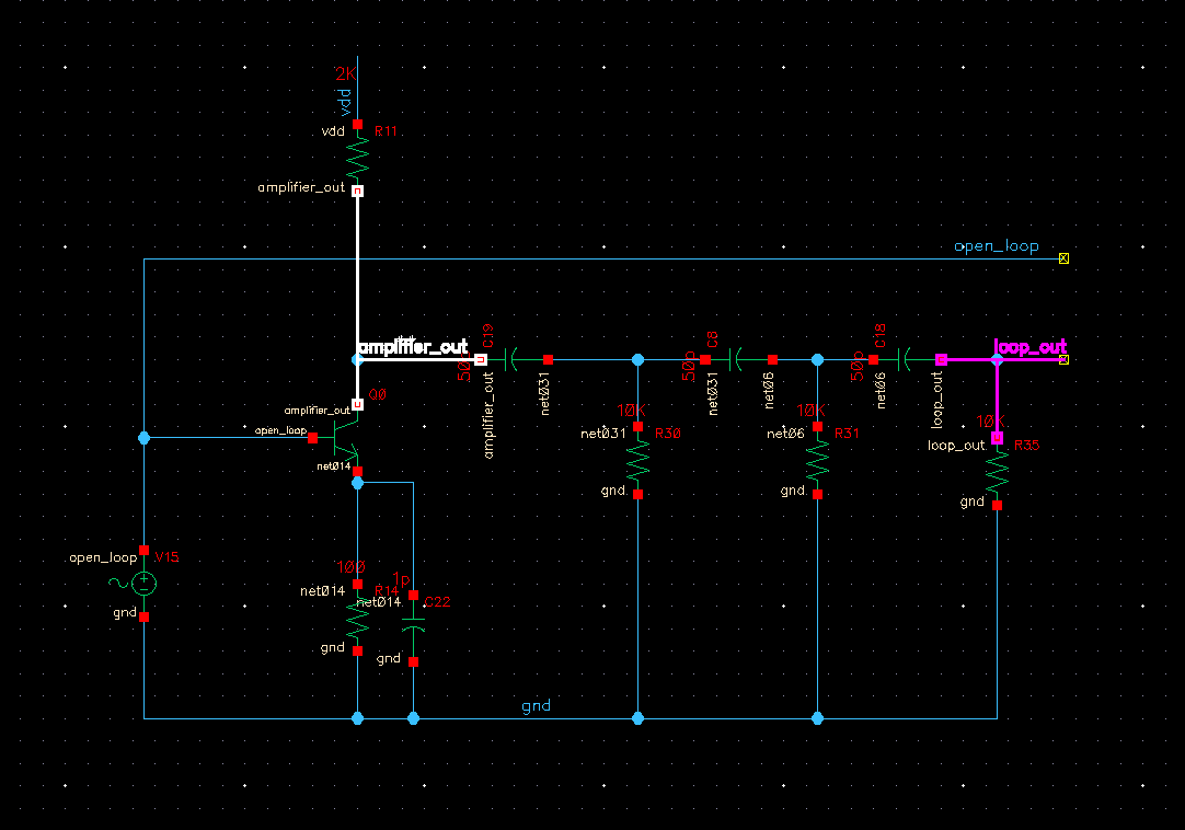
I am using 40nm PDK and i want to implement a RC oscillator of 1MHz using given npn pdk transistor.

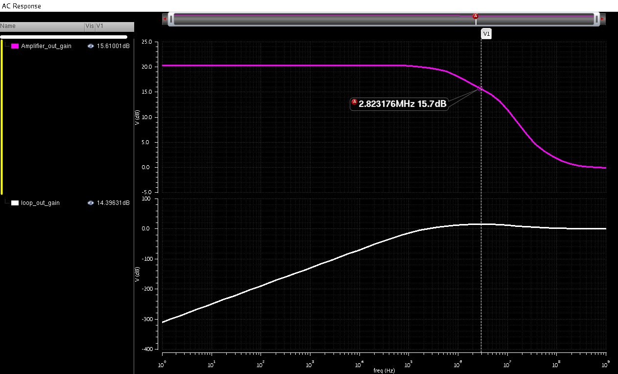
while setting Q-point i got that my transitor BW is ft = 2.7MHz.

and my supply voltage is 1.1V.

i am using conventional design of RC oscillator.

But my circuit doesn't start oscillatons. I dont know whether it is my initial conditions problem or circuit problem.

and i heard that for oscillator analysis HB simulation is better than transcient simulation. Is it true?

If so, how can i implement it in cadence?

please help..

thanks.


The problems with RC-phase shift oscillators based on a BJT amplifier are the input and output resistances of the amplifier (opamp: infinite input and zero output resistance).
Thus, it is not so obvious to fzlfill the oscillation condition (Barkhausen).
To solve your problem:

1.) provide a suitable base biasing (your circuit does not allow any DC current Ib);
2.) Start a proper loop gain analysis and check the oscillation condition.
 

Hi,

As you said i analyzed my loop.. i encountered a different behavior of the circuit.
that is, before connecting my feedback RC network the bandwidth of the amplifier looks promising. nearly 4MHz.

after connecting RC network the bandwidth is reduced to 8KHz.

Why this is happening and is this what you have said the output impedence problem?

I have attached the waveforms for your reference.

amplifier bandwidth without RC:


amplifier bandwidth with RC


the bandwidth of the RC circuit:


there must be some reason for this..

thanks.
 

Hi,

As you said i analyzed my loop.. i encountered a different behavior of the circuit.
--------------------

there must be some reason for this..

thanks.

It is not easy to help becaus I don`t know what you are showing us.
Loop gain? I don`t think so.
I assume that the last of the three figures shows the magnitude of the passive part (high pass) only, correct?

Did you correct the biasing circuitry?
 

I guess the loop gain is too small. Please try to add more 2 stages of amplifier.
 

The phase shift oscillator is finicky to get it going.

Recommendations:

Increase power supply to 4V or more.

Add a bit of bias current, adjusted through a potentiometer.

Reduce emitter resistor to a very low value. You may not need it at all.


Notice that precise adjustment is necessary, so that C1 attains equal ebb and flow of charge per cycle. If it does not do this, the circuit stagnates.
 

Hi.

this is my circuit..

with open loop


amplifier without RC network connected is,


and in my previous post first one is the bandwidth of my amplifier alone

second one is with RC network that is open loop gain.

and of course you are right with the third one.

What do you think is wrong in this?
thanks

- - - Updated - - -

The phase shift oscillator is finicky to get it going.

Recommendations:

Increase power supply to 4V or more.

Add a bit of bias current, adjusted through a potentiometer.

Reduce emitter resistor to a very low value. You may not need it at all.

My pdk transistor supports upto 1.8V only..

and what is ebb and how it affects oscillations...

thanks

- - - Updated - - -

I guess the loop gain is too small. Please try to add more 2 stages of amplifier.

hi

20dB is my gain and loop gain is very different nearly 2 dB.

How much gain needed for this oscillator.
thanks
 

My pdk transistor supports upto 1.8V only..

Does this mean you cannot have a power supply greater than 1.1V (referring to post #1)? This is very hard to believe regarding any simulator.

and what is ebb and how it affects oscillations...

C1 (in my schematic) must discharge an equal amount as it charges.
This happens every cycle.

'Ebb and flow' is a phrase we use for cyclical give-and-take action.

You must adjust the transistor bias so that it turns on sufficiently to discharge C1 a certain amount. Then the transistor must shut off (or almost shut off), so that C1 can charge an equal amount as it discharged.

There is only a narrow range of adjustment, where you can get the circuit to oscillate forever.
It is not difficult to make it ring for a few cycles at startup. There is a wide range where you can do that.
 

I guess the loop gain is too small. Please try to add more 2 stages of amplifier.

No - of course you can provide enough loop gain with one single stage only
However - kenambo, do you know the definition of loop gain? It is the gain of the COMPLETE loop (after opening it at a suitable point) including RC highpass and gain stage.
 

No - of course you can provide enough loop gain with one single stage only
However - kenambo, do you know the definition of loop gain? It is the gain of the COMPLETE loop (after opening it at a suitable point) including RC highpass and gain stage.

Yeah i knew that. and what exactly you mean by suitable point?

Because i opened my circuit after RC and given input to the transistor. Does this exhibit correct loop ?

and what is the reason for my gain reduction after adding the RC filter.

thanks.

- - - Updated - - -

My pdk transistor supports upto 1.8V only..

Does this mean you cannot have a power supply greater than 1.1V (referring to post #1)? This is very hard to believe regarding any simulator.

It is pdk dependent and i will try with your supply and share the results.

and how to give initial conditions for this circuit.

Because after that only i can fix the charging and discharging am i right.

thanks
 

Yeah i knew that. and what exactly you mean by suitable point?
Because i opened my circuit after RC and given input to the transistor. Does this exhibit correct loop ?

In your case (transistor oscillator) it is a problem to apply one of the simple methods for loop gain simulation because there is no point where a small output resistance
is connected to a much larger input resistance (example: opamp output always is a "suitable point).
Opening after the RC sections disconnects the transistor amplifier from the passive part.

That means: In your case, you should do the following:
As a first step, open the feedback loop and determine the small-signal (dynamic) input resistance r,in at the opening.
As a second step, load the passive part with this resistance r,in and perform the simulation.

As an alternative, you could load the passive part with a copy of the circuitry which you have disconnected.

Hi,

i understand what you said,
as you said i have just modified the circuit for measureing the open loop gain.

i have attached this and the outputs i got.

Is it correct or do i need to change something to measure the loop gain.
My schematic:


gain:


Phase:


thanks.
 

No - it`s not correct. Where is the copy at the opening?

Do the following:
1.) Open the loop and create two nodes A and B at the opening.
2.) Connect an ac source of 1V (against ground) to node B.
3.) Connect a mirror of the part of the circuit which was disconnected at node A.
4.) Perform an ac simulation and display magnitude (in dB) anf phase for V(B)/V(A).
 

Hi,

I measured my loop gain and it is nearly 5dB But what i got when i reviewed the phase is i couldnt get the phase shift correctly .. maybe this is the problem.

And another thing is my 60 deg phase shift of a particular frequency is not in the range of 3dB bandwidth of the RC filter.

and i found that at -3dB frequency my RC produces only 30 degree phase shift and for that my gain should be more nearly 30dB i presume.

so i combined 6 stages of RC to get 180 deg phase shift at -3dB bandwidth of my circuit.

Do you think i am going in a right way?

thanks
 

RC oscillator Ateenuation of RC network

Hi

While i am reading about RC oscillator, i came up with the line that specifies the RC network attenuation is 1/29th of the gain.

Where does this 1/29 come from?

and to avoid this our amplifier gain must be sufficient.

but how does it cause this attenuation?

thanks
 

Re: RC oscillator Ateenuation of RC network

Hi
While i am reading about RC oscillator, i came up with the line that specifies the RC network attenuation is 1/29th of the gain.
Where does this 1/29 come from?
and to avoid this our amplifier gain must be sufficient.
but how does it cause this attenuation?
thanks

Your RC network is of third order having a maximum phase shift of -270deg (for infinite frequencies).
Your oscillator consists of this passive 3rd-order network and an inverting amplifier. Because this amplifier produces a phase shift of -180deg
the RC network must produce additional 180deg to get in total a phase shift of -360deg (identical to 0 deg). This is the phase condition for oscillation.
Now - the magnitude of the passive network when the phase is -180deg can be calculated to be 1/29.
Hence, the inverting gain of the opamp must be -29 (in reality, for a safe start of oscillations: slightly above -29)
.
 
Where does this 1/29 come from?
The number is only valid for a specific RC circuit, unfortunately you forgot to mention it. I'm sure the number becomes obvious if you calculate the transfer function of the circuit.
 

my circuit is ordinary RC circuit with cadence ideal R and C devices.

And a different thing happens when i am connecting the RC circuit with my amplifier circuit.

I want more gain so used a three stage Amplifier... my circuit oscillates at a different frequency at which all of my ciruit's phase shift is zero.

that means my amplifier phase shift is zero in that frequency and my RC also gives zero phase for that frequency.

Is that even possible


thanks
 

that means my amplifier phase shift is zero in that frequency and my RC also gives zero phase for that frequency.

Is that even possible
Possible yes, but not necessary. More likely the amplifier phase will be compensated by a respective RC phase shift, resulting in 0 overall loop phase.

Also the oscillation condition must be fulfilled for both phase and magnitude.

It would be helpful if you show your recent circuit.
 

A three-stage amplifier? What kind of amplifier?
Did you consider that the input impedance of your amplifier must be considered for designing the whole circuit (it loads the passive RC circuitry)?
 

Status
Not open for further replies.

Part and Inventory Search

Welcome to EDABoard.com

Sponsor

Back
Top