Continue to Site

Welcome to EDAboard.com

Welcome to our site! EDAboard.com is an international Electronics Discussion Forum focused on EDA software, circuits, schematics, books, theory, papers, asic, pld, 8051, DSP, Network, RF, Analog Design, PCB, Service Manuals... and a whole lot more! To participate you need to register. Registration is free. Click here to register now.

Rail to rail input-output fully differential Op-Amp with class AB buffer driver

Status
Not open for further replies.
i didnt share the circuit not because i dont want to share it, but because i am not in the city of my university, however the setup from the gray is exactly the same setup i am performing, i am applying differential input voltage and sweeping it and getting the output.
I would like to see your simulation settings, the DC sources, internal and external device values, parameter settings, etc. I understand you tried to simulate that circuit, but the figure is not same as the test schematic with the elements in Cadence. For example how much are the feedback resistors? It is not added to the figure, but if they too low the gain can drop and output stage can leave the normal active region.
for sure at the non linear part of my graph some of them will be triode
And which is exactly in triode? Figure doesn't show it.
the non linearity you mentioned about with decreasing the loop gain is not the case of my situation since I am running dc simulation where the gain is highest, that what you talk about is when applying an ac signal with high frequency.
No. For every DC operating point, so for every DC input and output values the circuit has different small-signal model. This small-signal model can tell you how much is the DC gain too, not just the high-frequency gain. Think about Bode plot, which is an AC characteristic, but left side of the characteristic is basically the DC gain value, which is the loop gain's maximum value! Thus, if your amplifier devices are in triode region the gain from DC simulation and the maximum open-loop gain from AC simulation will decrease too.
but sine you you know the idea is from gray i can tell you that i did exactly as same he did in this picture but for my folded amp
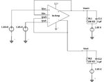
And how does it look like in Cadence? Are you using ideal devices? How the CMFB of this last circuit looks like? Many details are missing.
 
Dear Frank,

I could see your last comment from my email but it is not appearing here.

You gave me good point, I will run the dc operating point at the region where I am getting the non linearity to see which of the transistor is not in the saturation region.

You also asked me if my feedback resistor is loading my amplifier, actually I am simulating with very high resistors like 1 M Ohm. I was thinking the same as you so I then get confirmed by connected a buffer circuit as normal buffer , you can see it below please. I saw this setup with many papers and I wrote it for you using Visio.

I hope we could now make further discussion based on this setup

Thank you very much once again

dif_block_fully.jpg

- - - Updated - - -

Sorry I forgot to answer your last questions,

I am using a real transistor model from Europractice ,

concerning the CMFB, I am usin the one I already attacjed before and it is working very fine.

- - - Updated - - -

I am running the simualtion by this way,

from the DC simulation I am sweeping the X variable from -1.65 to +1.65 and recording the two output voltages as given in the circuit.
if you have a look you will see that increasing X will increase the voltage on Vin+ and decrease it on Vin- and vice versa, by this way I am applying true differential input
 

So, if I understood well you changed your test setup to the last circuit without feedback resistor dividers. That is good, it should work, and actually these differential-differential structures are used in this scenario only, where high input impedance is necessary. Do the DC operating point simulation you mentioned and we can discuss more after that.
And actually.... I don't see why did you designed a rail2rail buffer if you add in series with it a non-rail2rail circuit? And other thing is that the differential-differential circuit from post#20 can have very high gain. If you want to apply a feedback network around it and the series folded OPAmp, which also has a huge gain, I am sure it will oscillate.
And I am still suspicious that you are using only 1 CMFB circuit, I think you need 2. Tell me if I am wrong.
 
Dear frank,

Thank you very much for you active response to my post,

yes indeed I changed the setup to unity gain buffer configuration to be sure as you also suggested that it will not load my main amp.

I will do the DC when I be back then I will post the result.

Dear frank, the picture I showed of the differential difference amplifier I didnt connect it in series with my amplifier I shown in my early post, I used this image from Gray just to tell you that I am using the same principle.

For the CMFB, me too at the start was thinking that I need two CMFB, one at the upper side of the cascode stage of the folded amp and the other for the bottom side of the same cascode stage. However, Now I am only using one CMFB at the bottom and it is working perfectly.

Dear frank there is one point came to my mind regarding the simulation, I have shown you in my last simulation setup and result how I am varying a variable named X deferentially. So the plot you see from the simulation in the x-axsis is the variable X versus Vout+ and Vout- in the y-axis. this concept may lead us to the fact the I should multiply what I read from ICMR with factor two. Do you agree with this point ?

Thank you again
 

Status
Not open for further replies.

Part and Inventory Search

Welcome to EDABoard.com

Sponsor

Back
Top