Continue to Site

Welcome to EDAboard.com

Welcome to our site! EDAboard.com is an international Electronics Discussion Forum focused on EDA software, circuits, schematics, books, theory, papers, asic, pld, 8051, DSP, Network, RF, Analog Design, PCB, Service Manuals... and a whole lot more! To participate you need to register. Registration is free. Click here to register now.

R-2R digital to analog converter design

Status
Not open for further replies.

yefj

Advanced Member level 4
Joined
Sep 12, 2019
Messages
1,245
Helped
1
Reputation
2
Reaction score
3
Trophy points
38
Activity points
7,508
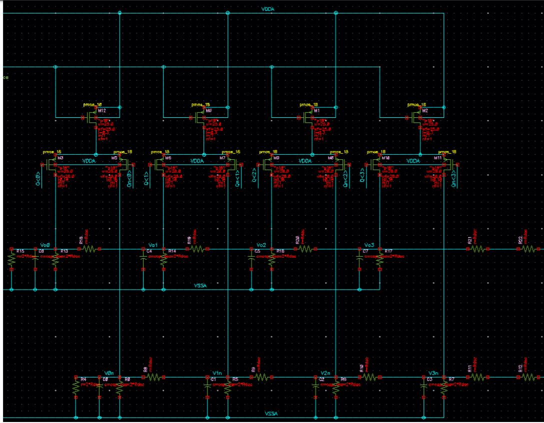
Hello, in the photo bellow i have a partial photo of analog implementation of a R 2R DAC.
However there is no exaplanation regarding why we need those lines of parallel capacitances and resistors.
I cant see where i connect the OPAMPS even.
I couldnt find this exact R-2R DAC there are many types.
If someone recognises this circuit configuration could you please post an article regarding such configuration?
Thanks.
3.JPG
 

Two possibilities. One is that these are "cpar" used
to model / anticipate layout parasitic effects on
settling time / glitch energy. Another is that these
are "slow-down" caps added explicitly to optimize
glitch behavior. Spikes carry a lot of RF energy that
may be best kept local (shorted to vssa through the
caps) so that intermodulation or simple pass-through
don't violate your amplitude-frequency mask.

Look to the instance master, to say which.
 

    yefj

    Points: 2
    Helpful Answer Positive Rating
Simulation of R2R network illustrates connections. The "counter IC" has 4 bits. The count is 0 to 15 therefore you can obtain 16 different volt levels.

Output pins provide paths internally to supply + and ground.
Final output is taken near the Most Significant Bit Q3.

DAC via R2R network 1k 2k resistors  4-bit counter.png


The bottom ground connection is necessary through the proper value resistor. Thus you obtain equal steps with each increment..
 
Last edited:

Your schematic appears to have mosfets as switching devices. This is not the same as a half-bridge which provides a path to supply + and to ground. Thus it causes your schematic to be more complicated, although that may be necessary if you wish to provide substantial current to a load.
 

Hello, do you know any full implementation with this lines so i could model it fully and understand how this whole thing works?
Thanks.
Two possibilities. One is that these are "cpar" used
to model / anticipate layout parasitic effects on
settling time / glitch energy. Another is that these
are "slow-down" caps added explicitly to optimize
glitch behavior. Spikes carry a lot of RF energy that
may be best kept local (shorted to vssa through the
caps) so that intermodulation or simple pass-through
don't violate your amplitude-frequency mask.

Look to the instance master, to say which.
 

Hello ,Could you help with some article with such implememtation ,so i could read and see how it works?
Thanks.
Your schematic appears to have mosfets as switching devices. This is not the same as a half-bridge which provides a path to supply + and to ground. Thus it causes your schematic to be more complicated, although that may be necessary if you wish to provide substantial current to a load.
 

Hello ,Could you help with some article with such implememtation ,so i could read and see how it works?
Thanks.

The R-2R arrangement is one of those clever inventions in electronics which rose to become widely used. It's an alternate method with a few advantages over the binary weighted resistor network.

An internet search turns up the following Youtube video about the R-2R ladder. Of course there's also benefit in playing with a simulation, to assist learning.

www.youtube.com/watch?v=Pc1aFloxSMw
 

Hi,

In post#1 you show a circuit of an IC design ... but you did not post in the "IC design" section.
Then you talk about Opamps....

Thus I'm a bit confused.
Do you really want to design your own IC ... with a DAC inside? .....or what else do you want to do?

Klaus
 

Hello KLaus, i am tried to find the general schematics of this whole analog circuit.
the R 2R structure, Where are the inputs where is the OPAMP goes there ,how to connect there RC structure?
The general view of the circuit as you think it should be.
Because i have only partial photo.whithout knowing those things.
Hi,

In post#1 you show a circuit of an IC design ... but you did not post in the "IC design" section.
Then you talk about Opamps....

Thus I'm a bit confused.
Do you really want to design your own IC ... with a DAC inside? .....or what else do you want to do?

Klaus
 

Status
Not open for further replies.

Similar threads

Part and Inventory Search

Welcome to EDABoard.com

Sponsor

Back
Top