Continue to Site

Welcome to EDAboard.com

Welcome to our site! EDAboard.com is an international Electronics Discussion Forum focused on EDA software, circuits, schematics, books, theory, papers, asic, pld, 8051, DSP, Network, RF, Analog Design, PCB, Service Manuals... and a whole lot more! To participate you need to register. Registration is free. Click here to register now.

Question regarding Power Supply Sequencing with TFT

FreshmanNewbie

Full Member level 6
Joined
May 10, 2020
Messages
386
Helped
0
Reputation
0
Reaction score
2
Trophy points
18
Activity points
3,857
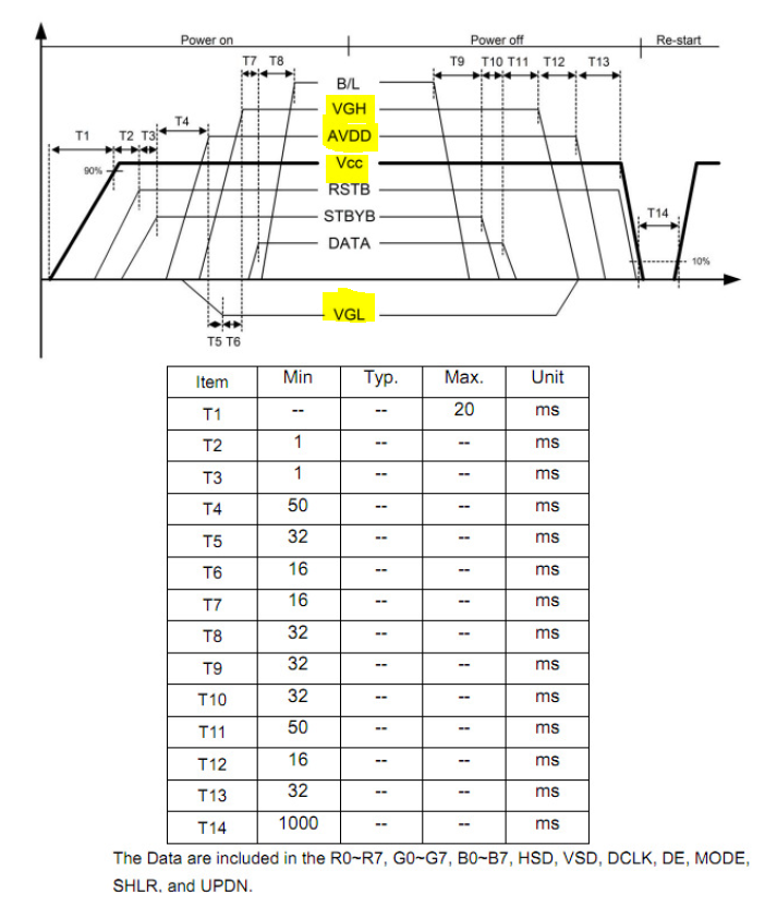
I have a TFT whose power sequencing is given below:
1698775213205.png


VGH (typ is 19V), VGL(typ is -10V), AVDD (typ is 12.4V), VCC (typ is 3.3V), are power supplies for the TFT.

Mentioned are the typ values required.

Would the TI part help to satisfy the power sequencing of the above TFT?
As far as I checked, in the TI datasheet, I plan to use as below, Vo1 for AVDD, Vo2 for VGL, Vo3 for VGH and Vo4 for Vcc.

Going through the power-up sequencing mentioned on page 12, section 7.4.1, it seems the TI part won't help with the power sequencing of the TFT.

Can someone confirm whether my understanding is correct? If yes, any workarounds, or suggestions possible?
 
It does support this sequencing.

"The device has two enable pins. These pins should be terminated and should not be left floating to prevent unpredictable operation. Pulling the enable pin (EN) high enables the device and starts the power-on sequencing with the main boost converter VO1 coming up first, then the negative and positive charge pump and the VCOM buffer"
If you can see the power sequencing for the TFT image, the sequencing is such that Vcc (which is 3.3V for the device) comes up first, then AVDD (12.4V), then VGL (-10V) and then only VGH (19V). Whereas, in the TI part, the Vcc (which is Vo4, 3.3V) comes last. How can it be supported? Can you please clarify?
 
I think you do not need Vo4 which requires Vi = 4.5 to 5.5V
Your 3.3V is the input Vi in the TI spec or called Vcc in the LCD spec.
Thank you for the clarification. So, I just have 2 more questions. So, I will give the Vcc to the LCD which will be the same as the Vi for the TI part and hence the power supply specification will be met. Thank you.

1. The TI datasheets, does not mention the time difference between the rising up of the Vox power supplies, right? I couldnt see in the datasheet. But the TFT datasheet has some timing values mentioned. How to cross check whether the rise time's or the on time of the TI output voltage would be matching the Display spec?

2. This board which has is connected to the display, will not have the MCU. The MCU is from another board which is connected to this board via a connector. In this case, how should I plan to give the data at the right delay time as mentioned in the TFT datasheet?

Thank you very much for your support.
 
1. This depends on your ability to follow the data sheet and then test and verify your ability to duplicate every recommendation then validate your design over temperature and voltage. The current limited charge pumps and undervoltage thresholds need to be understood along with Fig 14., soft start, enable ON/OFF response, load current, C tolerances and aging. Then ask TI tech support online in the TI forum with test results for any discrepancy.

2. This is your design challenge to ensure Power On Reset, Enable/disable and undervoltage detect and any interface conditions that might cause intermittent connection with power and a proper sequence of data and shared DC OK of 3.3V then your ability to include test points to verify your design expectations during DVT.

I have no experience with these chips. It would be wise to test the EVAL board then compare with your design.

Searching for more info resulted in this
 
Last edited:

LaTeX Commands Quick-Menu:

Similar threads

Part and Inventory Search

Welcome to EDABoard.com

Sponsor

Back
Top