talon
Newbie level 4
I am having trouble understanding gain in the single ended OTA case and its use in creating an op amp.
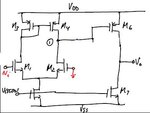
Say I have a first stage that is an OTA - diff pair with current source load. This diff pair has transistor M1 on the left and M2 on the right.
In small signal I input Vin at the left input of the diff pair and ground the right input. I take a single ended output at the drain of M2. Then the gain of this stage is positive(?)
A1 = gm1(ro4 || ro2)
I am unsure about the above result. The OTA should have output current Io = -GmVin with the output current Io point out towards the next stage but I am confused about where the negative sign comes from since increasing Vin causes current through M2 to decrease and the output node V1 to increase.
If my second stage consists of a common source amplifier with a current source at the source (implemented as a transistor) resulting in a gain of -gm6(ro6 || ro7) , then my total gain is
A1*A2 = -gm1(rop || ro2)gm6(ro6 || ro7)
Now if I disregard the necessary output stage for now (buffer), is what I have an op amp? Shouldn't the total gain be positive Vo=A(V+ - V-) where V+ is Vin and V- is grounded.
What is incorrect about my logic?
Thanks,
talon

Last edited: