Continue to Site

Welcome to EDAboard.com

Welcome to our site! EDAboard.com is an international Electronics Discussion Forum focused on EDA software, circuits, schematics, books, theory, papers, asic, pld, 8051, DSP, Network, RF, Analog Design, PCB, Service Manuals... and a whole lot more! To participate you need to register. Registration is free. Click here to register now.

Question about voltage supply for PLL

Status
Not open for further replies.

Hawaslsh

Full Member level 3
Joined
Mar 13, 2015
Messages
164
Helped
5
Reputation
10
Reaction score
7
Trophy points
1,298
Location
Washington DC, USA
Activity points
3,422
Hello,

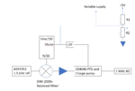
Picture2.png
We are working with a VCO and made a PLL work fairly well and cheaply on the bench, but in trying to transition to a stand alone device we ran into a problem. The block diagram is above, a mixer is used to downconvert the divide by 16 output of the VCO to a known reference (~ 1 MHz). The phase frequency detector (PFD) in the CD4046 is TTL, but the mixer output is AC coupled, so an op-amp is used to add a DC offset.
A large caveat to the whole thing, and the roof of the problem, for the VCO N/16 output to come near the 1.5 GHz reference, the Vcont on the VCO needs to be ~2.3V. Anything ± .4V and the frequency of the downconverted signal becomes too high for the op-amp and PFD. So, in order to "jump start" the loop we used a triple power supply (BK 1651). We set the +24V output to independent, and once the VCO output approached the reference, and the downconverted signal was below 32ish MHz, the loop took over.
In trying to move away from the bench, we tried the same idea with a voltage divider, but the lock was super unstable. Looking back on it, I'm not even sure why it worked attached to the power supply, I assume the output should have been regulated? There is a better way to solve this problem? Self admittedly, I know only what i've read about PLLs in the past month or so... so, not much.

Any insights would be appreciated.
 

Hi,

I've read your post several times now, but still are confused.

The phase frequency detector (PFD) in the CD4046 is TTL,
CD4046 is CMOS, not TTL.
If you want a TTL compatible 4046, then use 74HCT4046A. Or choose another logic family that meets your requirements.

but the mixer output is AC coupled, so an op-amp is used to add a DC offset.
OPAMPs are for analog signals, not digital signals.
To me it sounds you want to make an analog signal to become a digital signal.
If so, then use a comparator, no OPAMP. A comparator generates clean edges and clean logic levels.

the Vcont on the VCO needs to be ~2.3V.
What do you mean with "Vcont of the VCO" ... I can't find it in the datasheet.
I see it on your block diagram. Is it an output or input? Where does it go to or come from?

We set the +24V output to independent,
Where do you connect the 24V to?
And you mentioned "triple output" ... did you use the other two outputs, too? How?

we tried the same idea with a voltage divider
Where / how did you use a voltage divider?

******
Your headline talks about a "power supply problem" but still I don't see any power supplies in your block diagram nor can I relate it to the textual description. Am I missing something?

Please clarify.

Klaus
 

Thanks for taking the time to read the post several times! You are amazing to say the least.

CD4046 is CMOS, not TTL.
If you want a TTL compatible 4046, then use 74HCT4046A. Or choose another logic family that meets your requirements.

I dont really mind if its TTL or CMOS, i Just wanted to make the point the signal needed to be releveled to work with the PFD.

sounds you want to make an analog signal to become a digital signal.
If so, then use a comparator, no OPAMP. A comparator generates clean edges and clean logic levels.
I realize a sine wave into the PFD is far from ideal. I'm probably wrong here: can the same op-amp be used as a comparator (assuming its fast enough of course)?

What do you mean with "Vcont of the VCO" ... I can't find it in the datasheet.
I see it on your block diagram. Is it an output or input? Where does it go to or come from?
Capture.PNG
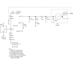
The VCO has a control voltage, vtune. Perhaps you were looking at the ADF4351? This control voltage is the issue. It is connected to both the BK 24V output and the output from the LPF (see pic below). We can remove the BK supply once the frequency difference between the 1.5 GHz reference and N/16 output is small enough to function within the amp and PFD bandwidth.

Where do you connect the 24V to?
And you mentioned "triple output" ... did you use the other two outputs, too? How?
In regards to the other outputs, the static +5V on th BK supply powers the HMC739 directly (both its analog and digital pins), and powers the remaining PLL components. The ADF4351 has its own 3.3v regulator which is powered from the static +5V. We dont use the second 24V output.

we tried the same idea with a voltage divider
Capture2.PNG
Originally we had Vtune, and subsequently the output from the loop filter, connected directly to the variable supply. That's where we figured we'd try the divider as a replacement. Leaving the divider ratio fixed, I tried a few resistor value combinations, mostly due to naivety, to no real affect. As mentioned before, I'm not entirely sure why it worked at all when connected to the variable supply.

Your headline talks about a "power supply problem"
Hopefully the picture above better illustrates. However, please let me know if any additional info would help. Due to world events, it has been 100% toddler time for the past few weeks.. its hard to find time to be detailed, let alone form coherent thoughts.

Perhaps I'm doing this all wrong and trying to create the actual PLL my self. It was certainly a good learning exercise, but needlessly painful and ultimately noisy? Analog devices makes a much more narrow band PLL in the 24 GHz range, and it works in conjunction with a second synthesizer which does the PLL. The ADF4159 is quite wide band and expensive, I'm going to check now, but I assume they make much more narrow band, cheaper synthesizers for these purposes, specifically 1.4-1.55 GHz.

thanks

- - - Updated - - -

ADF4152A seems like a reaonsible replacement to, basically everything, but the VCO and a loop filter. And its less than 3 bucks, not bad.
 

Hi,

(Please don't be scared by my lengthy post, I just wat to explain my thinking)

I dont really mind if its TTL or CMOS, i Just wanted to make the point the signal needed to be releveled to work with the PFD.
To get stable output and to get a reliably running circuit you need to choose the right IC (and family) and keep on the ICs specifications.
Honestly it's hard for me to find out the input signal requirements in old CD4046 datasheet. Since we don't have the complete schematic I don't know which signal with which levels and waveform you feed to which IC and pin.

I'm probably wrong here: can the same op-amp be used as a comparator (assuming its fast enough of course)?
An Opamp is an Opamp, a comparator is a comparator, each desined for it's job. Sadly they use the same schematic symbol, but the function and requirements are different.
There are several threads here (and in the internet) discussing the difference.
In short:
* Opamp
analog input, analog output. Negative feedbacked. Differential input voltage should be almost zero to avoid input stage saturation, output voltage should never become saturated at the supply rails. Else they come out of regulation which causes extra delay, in worst case phase reversal.
* Comparator:
analog input, digital output. Not negative feedbacked, maybe positive feedbacked. No analog regulation loop. Differential input voltage may be big, input stage is designed not to get saturated. Output stage is desiged to go to the supply rails (no must). They generate output with fast edges. No phase reversal.

The VCO has a control voltage, vtune.
We live in different countries, have different languages, you have all the background knowledge about your application, we not.
When you use different names and terminology as in the datasheet, then maybe you get wrong response..

This control voltage is the issue. It is connected to both the BK 24V output and the output from the LPF (see pic below). We can remove the BK supply once the frequency difference between the 1.5 GHz reference and N/16 output is small enough to function within the amp and PFD bandwidth.
In your new block diagram the Vtune is connected to the both the 24V supply and the 5V voltage divider.
I assume this is optional connection...

If I understand correctly, then in case the VCO output frequency becomes too high and the PFC refuses to work. It can't lock

If so, then I see some options:
* use a faster PFC ( 74HC4046 is about 10 times faster than CD4046)
* ramp up Vtune slowly enough that the PLL safely can lock. This can be done by a slow RC, maybe with the help of diodes.
My idea: on power down the C gets discharged by a diode. On power up the C charges slowly ... limiting the Vtune voltage.
Then at some point (close to the desired VCO frequency) the LPF output takes over and the PLL should lock.

Klaus
 

(Please don't be scared by my lengthy post, I just wat to explain my thinking)
to the desired VCO frequency) the LPF output takes over and the PLL should lock.
Klaus

On the contrary, I appreciate you taking the time to help!!

Looking through the analog device website they have a PLL chip that would work with the VCO's divide by 16 output. Also, both parts exist in their free PLL design software, making it seem all too simple.
Capture.PNG

it would be cheaper, few parts, and probably function better than my thrown together PLL.

Thanks again for all your time!
 

But HMC739 is not PLL controlled, how will you overcome the Drifting Problem by Temperature ??Even you use a fixed Vtune voltage, the VCO of HMC739 will drift..
Your Loop Approximation is not very healthy..
 

Status
Not open for further replies.

Similar threads

Part and Inventory Search

Welcome to EDABoard.com

Sponsor

Back
Top