Continue to Site

Welcome to EDAboard.com

Welcome to our site! EDAboard.com is an international Electronics Discussion Forum focused on EDA software, circuits, schematics, books, theory, papers, asic, pld, 8051, DSP, Network, RF, Analog Design, PCB, Service Manuals... and a whole lot more! To participate you need to register. Registration is free. Click here to register now.

question about Gate driver in buck converter!!!!!

Status
Not open for further replies.

nelly1

Junior Member level 3
Joined
Jun 14, 2012
Messages
29
Helped
0
Reputation
0
Reaction score
0
Trophy points
1,281
Activity points
1,495
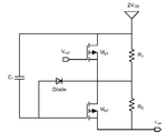
Here is a topology presented by Sean R.Bradburn.

For high-side gate driver, when the switches are off, source voltage of Mp2 will fall to VDD. C1 discharges through diode.

But !!!!!!!!

why the gate voltage of Mp2 will fall further below its source voltage through diode???
Someone please help!!!!!!!!!!!!
p2.5.png
 

So question, is Mp1 and Mp2 pfets? also are you stating both are switches or mp1 is switch or you have other switches not shown?
Consider this a bump back into the questions.
-Pb
 

This is a high side switch using device stacking to
get more than the individual device Vds rating.

The diode is for pumping C1, to establish the cascode
gate bias for MP2. I suppose there is some benefit to
energizing the R1/R2 divider for only the low portion
of the cycle, but to me it's trivial and I'd just (and
have) connect the tail to the negative (ground) rail.
 

yes, MP1 MP2 are both pfets and use as switches. They are stacked as high-side part. What is bump back your mean??

- - - Updated - - -

because of the power comsunption, i only want this divider for low portion of the cycle. and i thought this questions might caused by some leakage in MP2, not due to the source terminal voltage of Mp2
 

Status
Not open for further replies.

Similar threads

Part and Inventory Search

Welcome to EDABoard.com

Sponsor

Back
Top