Continue to Site

Welcome to EDAboard.com

Welcome to our site! EDAboard.com is an international Electronics Discussion Forum focused on EDA software, circuits, schematics, books, theory, papers, asic, pld, 8051, DSP, Network, RF, Analog Design, PCB, Service Manuals... and a whole lot more! To participate you need to register. Registration is free. Click here to register now.

[SOLVED] Quad Cross couple PTAT bandgap reference generatorworking principle

Status
Not open for further replies.

sawakita

Newbie level 5
Newbie level 5
Joined
May 14, 2013
Messages
8
Helped
0
Reputation
0
Reaction score
0
Trophy points
1,281
Visit site
Activity points
1,374
PTAT quad cross couple.PNG

Hi good day,

If someone could please explain to me this circuitry working principle. I have search many books and articles but havent really find any answer to my question.

I understand how the bandgap reference circuit works and the principle. I can understand the typical bandgap reference circuit.

But I have problem where there's a cross couple circuitry involves.

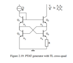
based on the picture attached,

I dont understand how the currents flows in this circuitry especially at the cross coupled based.

I understand the current mirror on top and that both currents flows at Q3 and Q1,

my question is let say Q4 is off, so current from Q3 flows to base of Q2 turning on Q2,

that means current from Q1 is shorted to ground when Q2 is turned on.

that means currents from Q1 would never flows to base of Q4 because Q2 is always on due to Q4 always off.

so in this case how does Q4 activate?

to generate PTAT both Q2 and Q4 needs to turn on to get the delta_vbe.

I have search in this threads the answer but couldnt find any.


Thanks in advance for the explaination.
 

Usually, please some one correct me if I am wrong, there are two stable states for this kind of circuits. Depending on the initial conditions the circuit could go to a state where the current is zero, so for this reason some sort of start up circuitry is needed.
 

Usually, please some one correct me if I am wrong, there are two stable states for this kind of circuits. Depending on the initial conditions the circuit could go to a state where the current is zero, so for this reason some sort of start up circuitry is needed.


Thanks for the reply.

From what i read, this PTAT generator is self biased (I think maybe no startup biased is needed but Im not sure)

Also for PTAT generator to works both Q2 and Q4 need to turn on. It has something to do with translinear principle from what I have researched where in the explaination the current flows to both sides,

but I still have difficulties to understand why it flows in both sides of the circuitry
 

I agree that the circuit is self biased, doesn't need a startup means. But the expression for the output current can't be right, it also depends on the input current.
 
  • Like
Reactions: tpetar

    tpetar

    Points: 2
    Helpful Answer Positive Rating
I understand the current mirror on top and that both currents flows at Q3 and Q1,

my question is let say Q4 is off, so current from Q3 flows to base of Q2 turning on Q2,

that means current from Q1 is shorted to ground when Q2 is turned on.

I also believe that the base currents were neglected in obtaining the result Vt/Rln(A1A4/A2A3)
 

I agree that the circuit is self biased, doesn't need a startup means. But the expression for the output current can't be right, it also depends on the input current.

Hi FvM

From what i read this circuit works in the end independant of input current, and depends mainly on the emitter area, normally in example 4:1 with Q4 emitter area is larger.

but I still cant figure out how the circuit works where currents flows to both sides, it should be just either through Q2 or Q4

thanks for the reply

- - - Updated - - -

sorry i should add Q1 and Q3 are matching with emitter ratio 1:1

while Q2 and Q4 4:1 with Q4 the larger emitter area.

I think the answer has something to do with the emitter area different ratios
 

Usually, please some one correct me if I am wrong, there are two stable states for this kind of circuits. Depending on the initial conditions the circuit could go to a state where the current is zero, so for this reason some sort of start up circuitry is needed.

There can be a third stable state, if you close the loop
with a high side feedback mirror - that is, the transistors
may enter saturation and stay in a much higher current
state, if kicked by noise or some electrical anomaly.
For this reason it's good to have a resistive current
limited in one leg that is sufficient to keep devices
below the onset threshold, for this.

Seen this in real life, on older bipolar technology.

Now having a PTAT that depends on you already having
an ideal current source, is not the most helpful thing....

If im not mistaken u mean to say that should the current goes high enough through Q4 while Q2 is off, the high currrent causes high drop at emitter resistor, limiting vbe of Q4 eventually shutting off Q4 when vbe is less that turn on voltage, which makes current from Q3 flows to base of Q2 now that Q4 is off.

so its some kind of a safety mechanism, I did think of this before, but then I wonder how the circuit switch back Q4.

on the other hand the circuit also works with current flowing on both sides.

it is an old bipolar technology which im currently working on :)
 

I don't understand which problems you have in analysis of circuit operation. Q1/Q3 will enforce a certain range of Q2/Q4 collector voltage and cause a negative loop gain of the cross coupled pair. This results in one stable operation point of the circuit.

The question about the apparently wrong expression for Iout still holds.

Im sorry. Its a bit difficult for me to follow. Can you please explain based on my first post. What do you mean by negative loop gain.

Just imagine like u are teaching this circuit to me. No need any formula. Just want to know how it works and why.
Why does it not cause complete short at Q2 and why Q4 not completely off when Q2 is on for example.

Thanks for ur help and explaination
 

If you neglect the base currents, PTAT current expression comes as follows:
Same current I flows through Q1 and Q2, So

Vbe1 - Vbe2= Vt ln(A3/A1) , where Vbe1 is the base -emitter voltage of Q1 and like wise.

or Vb1 -Ve1 -Vb2+Ve2=Vt ln(A3/A1) or Vb1-Ve1-Vb2=Vt ln (A3/A1)

Similarly for Q3 and Q4 following equation can be written
Vb3 -Ve3 -Vb4+Ve4=Vt ln(A4/A2)


Vb1=Vb3 , Ve1=Vb4, Ve3=Vb2 , subtracting the above two equations give Ve4=Vt ln(A1*A4/A2A3)

So the PTAT current is Vt ln(A1*A4/A2A3)/R
 
Last edited:
  • Like
Reactions: FvM

    FvM

    Points: 2
    Helpful Answer Positive Rating
hi Sawakita,
writing a kvl we see that: Vbe1+Vbe4+R*Iout=Vbe3+Vbe2 if we choose appropriate transistor areas and appropriate R, usually R*Iout is much less than Vbe (maybe around 50-100mvolt) therefore neglecting R*Iout in this relation we can conclude that turning on 3 of the transistors will force the forth one to turn on.
Moreover assume that as you said Q4 is off. this is not the normal operation of the circuit therefore a large current will flow through base of Q2 which will increase Vbe2 dramatically this increase in Vb2 (assuming that the Iout has not changed and so Vbe3 has not changed yet ) will increase Vb3 and consequently Ve1 which is also Vb4. therefore Q4 will turn on and will steal some current from base of Q2. and after the transients are finished the circuit will have its normal and expected operation.


Hi Mahdi3999,

thanks for the circuit description, this might be the one im looking for. just something im not sure of:

why do u say this

" therefore neglecting R*Iout in this relation we can conclude that turning on 3 of the transistors will force the forth one to turn on. "

why is it when we neglect R*Iout, turning on 3 would would force 4 to turn on as well.

thanks again for the reply
 

R*Iout is always present in the KVL relationship but as I said it may be in the order of 50-100mvolt which is much smaller than Vbe(=700mvolt). Just in order to have a simplified case, I neglected R*Iout in Vbe1+Vbe4+R*Iout=Vbe3+Vbe2. then we'll have Vbe1+Vbe4=Vbe3+Vbe2. Imagine that all the transistors except Q4 are on(Vbe1,2,3=700mvolt) then according to the KVL, Vbe4=700mvolt that is Q4 is on too.
 

R*Iout is always present in the KVL relationship but as I said it may be in the order of 50-100mvolt which is much smaller than Vbe(=700mvolt). Just in order to have a simplified case, I neglected R*Iout in Vbe1+Vbe4+R*Iout=Vbe3+Vbe2. then we'll have Vbe1+Vbe4=Vbe3+Vbe2. Imagine that all the transistors except Q4 are on(Vbe1,2,3=700mvolt) then according to the KVL, Vbe4=700mvolt that is Q4 is on too.


hi thanks for the reply.

I think now I understand and I agree. so the explaination must be supported by formula as well.

question regarding ur previous explaination.

" this is not the normal operation of the circuit therefore a large current will flow through base of Q2 which will increase Vbe2 dramatically this increase in Vb2 (assuming that the Iout has not changed and so Vbe3 has not changed yet ) will increase Vb3 and consequently Ve1 which is also Vb4. therefore Q4 will turn on and will steal some current from base of Q2. and after the transients are finished the circuit will have its normal and expected operation.
"

for the highlighted red i supposed it can be explained by formula if Ibase high => vbe will also increase.

and then can u explain further on this:

" consequently Ve1 which is also Vb4. therefore Q4 will turn on and will steal some current from base of Q2 "

I agree Ve1 is Vb4, but at this moment Q2 is on, so vb4 cannot turns Q4 on, all the current from Q1 should flow straight to gnd through the on of Q2, meaning ve1 should be gnd potential, hence vb4 is also gnd potential, meaning Q4 should be off

i guess u meant to say Q2 and Q4 is turn on at the same time meaning the current flows through Q2 and base Q4. but how can tht be when Q2 is now a short. my question is why Q4 would on according to u when Q2 should shorted all the current completely to gnd.

sorry for kept asking question. just really want to understand this.

thanks for ur reply.
 

I think, the error in reasoning is to imagine the transistors as switches that are on or off. They are analog parts with a continuous characteristic. In some circuits, transistors are combined in a way that they create bistable behaviour, the operation point will fall to one or the other side. This is happens if positive feedback dominates.

Positive feedback is present in a cross-coupled circuit, so you might doubt at first sight about stable behaviour. But it turns out that negative feedback, or more exactly the low emitter output impedance of the upper transistors is stronger here. You'll see that any arbitrary operation point converges against one stable point.
 

    V

    Points: 2
    Helpful Answer Positive Rating
I agree Ve1 is Vb4, but at this moment Q2 is on, so vb4 cannot turns Q4 on, all the current from Q1 should flow straight to gnd through the on of Q2, meaning ve1 should be gnd potential, hence vb4 is also gnd potential, meaning Q4 should be off

i guess u meant to say Q2 and Q4 is turn on at the same time meaning the current flows through Q2 and base Q4. but how can tht be when Q2 is now a short. my question is why Q4 would on according to u when Q2 should shorted all the current completely to gnd.

sorry for kept asking question. just really want to understand this.

thanks for ur reply.

I answered your question from voltage point of view. you can explain it from current point of view too. if Ve1 is at ground potential(acctually it will never be ground, at the extreme it can be Vce,sat which can be about 0.2volt) then Q2 sinks a current much much larger than what Q1 can provide. in this case, Ve1 is for example 0.2volt, then since Q1 is on, Vb3 must be about 0.9volt while Ve3 is 0.7volt(since Q2 is on) therefore under these circumstances Q3 will be off and then the circuit will go back to its expected operation(because Q3 made Q2 to sink that large current now we see that a large Q2 current will force Q3 to turn off ).
 

    V

    Points: 2
    Helpful Answer Positive Rating
I answered your question from voltage point of view. you can explain it from current point of view too. if Ve1 is at ground potential(acctually it will never be ground, at the extreme it can be Vce,sat which can be about 0.2volt) then Q2 sinks a current much much larger than what Q1 can provide. in this case, Ve1 is for example 0.2volt, then since Q1 is on, Vb3 must be about 0.9volt while Ve3 is 0.7volt(since Q2 is on) therefore under these circumstances Q3 will be off and then the circuit will go back to its expected operation(because Q3 made Q2 to sink that large current now we see that a large Q2 current will force Q3 to turn off ).

Hi FvM

I agree with you, people has been telling me i need to just see it that its stable. i guess its just me adamant enough to press on. its easier to remember this vcircuit behaviour when i can understand it in a chronologically way though i doubt ill forget this circuit now. thanks for your reply.

Hi Mahdi,

I can use ur explaination too :) I forget the Vce 0.2V, in that case of cause it is not totally shorted. because in circuit analysis ive only seen they would consider vbe only as voltage drop for on transistor.
from voltage point of view it make sense from the formula, when three transistor on the last one would also be turned on ignoring V_R at emitter Q4, mathematically proven so to say.

thanks for ur help guys !!
 

FvM,

Easiest way to analyze the output current, IMO, is to ignore all the unnecessary terms (Vt, Is), since all the transistors will be at the same temperature and have scaled saturation currents anyway. So the Vbe for a 1x transistor is ln(Ic) and for a 4x transistor is ln(Ic/4).

Then with KVL around the translinear loop (where Q1 and Q3's bases being tied together forces the voltages to add up),
\[V_{BE1}+V_{BE4}+I_{OUT}*R=V_{BE2}+V_{BE3}\]
Thus,
\[\ln(I_{IN})+\ln(\frac{I_{OUT}}{4})+I_{OUT}*R=\ln(I_{IN})+\ln(I_{OUT})\]
Cancelling ln(Iin) and ln(Iout),
\[-\ln(4)+I_{OUT}*R=0 => I_{OUT} = \frac{\ln(4)}{R}.\]
Beta-dependent error terms exist, causing an Iin dependence, but to first-order it's correct.

Can you explain how its stability is evaluated? Often the cross-coupled structure of Q2/Q4 is used as a latch; I'm thinking the loop gain is normally gm*ro*gm*ro (i.e., huge and positive) and therefore the bistable, latching behavior. Here however, we have Q2/Q4 feeding a low differential-mode impedance (high common-mode impedance, but that's irrelevant): Q2's gm is equal to Q1's gm, so Q2/Q1 acts as a unity gain amplifier from Q2's base to Q1's emitter, while Q3/Q4 act as a slightly-less-than-unity-gain amplifier (since Q3 is degenerated by R). Then, cross-coupling them yields a loop gain of less than unity, and therefore it's stable. Does this seem about right? From this I'd say the cross-quad, therefore, is playing on the edge of stability if there is no emitter degeneration; stability can only be assured if emitter degeneration has been added.

-- Edit --

How embarrassing, in my zeal for removing "unnecessary" terms I posted an erroneous equation! Specifically, it was the removal of the Vt terms that was in error. The last equation of my post, instead of reading Iout=ln(4)/R, should be Iout=Vt*ln(4)/R (d'oh, it's a PTAT current!). Ignoring Vt terms obviously isn't so great for PTAT generators.

Thankfully, I caught this error before anybody else =)
 
Last edited:

monsoon has shown the equations for "ideal" transistors with infinite current gain in post #11. He already convinced me about independence of output from input current. I didn't further comment on it because it's not the primary problem addressed in the original post.

Regarding stability considerations. I think the circuit is not on the stability edge, there's a negative feedback mechanism not considered in your post.

You state that common emitter stage loaded with a transistor in common collector configuration has about unity gain. So you would get +1 gain for a symmetrical cross coupled structure and hopefully < +1 with degeneration. But for a stable operation point, the structure needs overall negative DC loop gain, which can't be explained with the simple cross coupled structure.

I see, that I also didn't clearly hit the point in my previous posts. I think it's the coupling through the Q1/Q3 base node that creates the negative feedback.
 

Status
Not open for further replies.

Similar threads

Part and Inventory Search

Welcome to EDABoard.com

Sponsor

Back
Top