Continue to Site

Welcome to EDAboard.com

Welcome to our site! EDAboard.com is an international Electronics Discussion Forum focused on EDA software, circuits, schematics, books, theory, papers, asic, pld, 8051, DSP, Network, RF, Analog Design, PCB, Service Manuals... and a whole lot more! To participate you need to register. Registration is free. Click here to register now.

[SOLVED] purpose of Resistors and Capacitors in CMOS inverter as a small signal amplifier

Status
Not open for further replies.

esteemera

Newbie level 2
Joined
Aug 16, 2013
Messages
2
Helped
0
Reputation
0
Reaction score
0
Trophy points
1
Activity points
22
CMOS inverter as amplifier.png

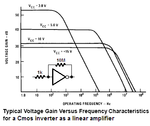
In the attachment, capacitors and high value resistors have been used. What is the purpose? Is it to minimize distortion and maintain the stability in the mid frequency band?
I don't have software's to try simulate and check the result. Any thoughts on the output of the amplifier for different resistor or capacitor values?

Thanks.
 

The capacitors are for DC-blocking, the bias voltage
source attempts to put the inverter at the center of
the linear region and the resistor prevents signal
attenuation. It's better as a rule to just autobias the
inverter from its own output, or from a dummy, to
get away from process sensitivities.

This is likely a poor-boy RF input amp or something
like that.
 
Esteemera, I am sure that your circuit will nor work in practice because the circuit never will find a suitable bias point around half of the supply voltage.
Instead, use a large resistor R2 between output and input (100% dc feedback).
More than that, you need a coupling capacitor to inject the input signal. More than that, you should use an additional series resistor R1 to fix signal gain. Otherwise, the gain depends on the load R2 and the (unknown) differential output resistance of the CMOS pair.
 
Last edited:

capacitors are used to block dc and allow ac, it acts as a filtering agent.resistors are used as conducting ad discharging element to discharge the excess amount of heat generated during circuit operation towards ground thereby protecting the circuit.
 

If the Cmos "amplifier" has only 5V for its power supply and it is a Cmos IC like a CD4069 then its voltage gain is about 100 with no load. But when its output level is near the rails then its distortion is very high.

Usually its input is auto-biased from its output and it is inverting like this:
 

Attachments

  • Cmos amp.PNG
    Cmos amp.PNG
    18.6 KB · Views: 89

capacitors are used to block dc and allow ac, it acts as a filtering agent.resistors are used as conducting ad discharging element to discharge the excess amount of heat generated during circuit operation towards ground thereby protecting the circuit.

Are you sure about the purpose of the resistors ???
 

resistor dissipates energy in the form of heat
 

I am assuming that this is from a test paper, or some such :) -

C1 couples the A.C. (sinewave?) signal generator output, V3, to the circuit and C1 blocks the d.c. voltage V1 from reaching this generator.
Bias to the 2 FETs (M1 and M2) gate connections, is supplied by battery V1 via current limiting resistor R1.
A large value R1 is used as FETs (M1 and M2) require very small currents to bias them on, and to form a high pass filter with C1.
Assuming the battery V1 has negligible resistance, then C1 and R1 make a high pass filter with 6db/octave rate, and a -3db point at about 10Hz.
The 5volt battery, V2, is the main supply for the FETs (M1 and M2) circuit.
The FETs (M1 and M2) have no feedback applied to them. This results in the FETs (M1 and M2) amplifying at their full gain and so would clip the A.C (sinewave?) on their output.
The output at resistor R2 would be a squarewave of the same frequency as the A.C signal generator V1.
C2 couples the output of the FETs (M1 and M2) circuit to load resistor R2 forming another high pass filter, while blocking any D.C component at this point.
C2 and R2 form another high pass filter with a 6db/octave rate and a -3db point at 100Hz.
C4 and R2 form a low pass filter with a -3db point at about 340kHz.
The output waveform would be a squarewave with slightly rounded rising and falling edges from 100Hz to about 300kHz, from about 338kHz and above the output would diminish at a 6db/octave rate, becoming more 'rounded' or sinewave-like as the frequency rises.

Hope that near it's very early in the morning where I am right now so please check the figures that I've done 'back of the envelope' style 8-O calculations.
 
It worked for the purpose to prove something. Thank you for your response.

- - - Updated - - -

I am assuming that this is from a test paper, or some such :) -

C1 couples the A.C. (sinewave?) signal generator output, V3, to the circuit and C1 blocks the d.c. voltage V1 from reaching this generator.
Bias to the 2 FETs (M1 and M2) gate connections, is supplied by battery V1 via current limiting resistor R1.
A large value R1 is used as FETs (M1 and M2) require very small currents to bias them on, and to form a high pass filter with C1.
Assuming the battery V1 has negligible resistance, then C1 and R1 make a high pass filter with 6db/octave rate, and a -3db point at about 10Hz.
The 5volt battery, V2, is the main supply for the FETs (M1 and M2) circuit.
The FETs (M1 and M2) have no feedback applied to them. This results in the FETs (M1 and M2) amplifying at their full gain and so would clip the A.C (sinewave?) on their output.
The output at resistor R2 would be a squarewave of the same frequency as the A.C signal generator V1.
C2 couples the output of the FETs (M1 and M2) circuit to load resistor R2 forming another high pass filter, while blocking any D.C component at this point.
C2 and R2 form another high pass filter with a 6db/octave rate and a -3db point at 100Hz.
C4 and R2 form a low pass filter with a -3db point at about 340kHz.
The output waveform would be a squarewave with slightly rounded rising and falling edges from 100Hz to about 300kHz, from about 338kHz and above the output would diminish at a 6db/octave rate, becoming more 'rounded' or sinewave-like as the frequency rises.

Hope that near it's very early in the morning where I am right now so please check the figures that I've done 'back of the envelope' style 8-O calculations.

Thanks exactly what I needed. Although like you mentioned the first two figures are off by a decimal nevertheless very good explanation.

- - - Updated - - -

There should be a special forum for students who know nothing about electronics.

I'm sure we wouldn't mind as long as we get correct explanation/answers.
 

Status
Not open for further replies.

Similar threads

Part and Inventory Search

Welcome to EDABoard.com

Sponsor

Back
Top