Continue to Site

Welcome to EDAboard.com

Welcome to our site! EDAboard.com is an international Electronics Discussion Forum focused on EDA software, circuits, schematics, books, theory, papers, asic, pld, 8051, DSP, Network, RF, Analog Design, PCB, Service Manuals... and a whole lot more! To participate you need to register. Registration is free. Click here to register now.

Pspice AC analysis of converter problem

Status
Not open for further replies.

dracarys99

Newbie level 5
Joined
Nov 13, 2020
Messages
10
Helped
0
Reputation
0
Reaction score
0
Trophy points
1
Activity points
109
I want to get the bode plot of the converter. For this I'm trying to do the AC analysis by voltage injection and I used an average switch model. It is a ZCS buck converter, the elements added for ZCS is L2 and C2. I intend to take the loopgain = dB(Voltage across V5).
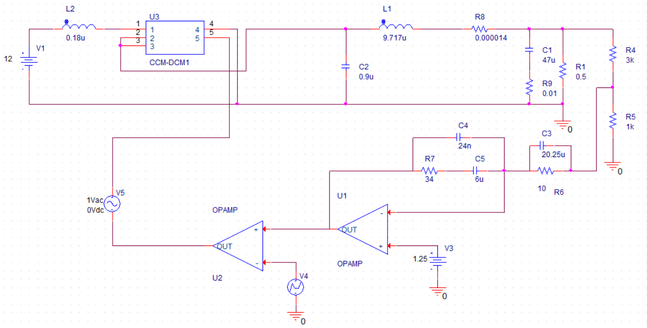
1614780749324.png


I keep getting the "Convergence problem in bias point calculation" error. What am I doing wrong here?
 

I keep getting the "Convergence problem in bias point calculation" error. What am I doing wrong here?
You don't need to determine the initial bias point, so try the simulation skipping the initial operating point calculation (.uic command).
 

You don't need to determine the initial bias point, so try the simulation skipping the initial operating point calculation (.uic command).

Thanks for the reply. But I used the "AC Sweep/Noise" analysis type. I think the option you mentioned is only there in the transient analysis. Or should I be using the transient analysis for this purpose?
 

Why is U2 there? Having a comparator (with near-infinite gain) in the feedback loop is going to make finding a stable operating point impossible.

I would start by removing the feedback portion entirely and just doing open loop simulation first.
 

It's not possible to derive the loop gain of a switched mode converter in AC analysis.
 
To use AC analysis (which you need to generate a Bode plot) on a switch-mode circuit you have to convert the PWM modulator (U3) to a linear gain block (assuming its transfer function is reasonably linear) with gain equal to the change in the PWM average output voltage divided by the change in error voltage at the modulator input.
Thus, for example, if a 2V change in the PWM input control voltage varied the PWM duty-cycle from 0% to 100%, and 12V was being switched, then the linear gain of the PWM modulator is 12V/2V = 6V/V.

Make sense?
 

It's not possible to derive the loop gain of a switched mode converter in AC analysis.
To use AC analysis (which you need to generate a Bode plot) on a switch-mode circuit you have to convert the PWM modulator (U3) to a linear gain block (assuming its transfer function is reasonably linear) with gain equal to the change in the PWM average output voltage divided by the change in error voltage at the modulator input.
Thus, for example, if a 2V change in the PWM input control voltage varied the PWM duty-cycle from 0% to 100%, and 12V was being switched, then the linear gain of the PWM modulator is 12V/2V = 6V/V.
I believe this is the purpose of the "CCM-DCM1" block. It's a state space average model of the switching components. I've never used this method myself though.
 

Anyways, while this may work fine for hard switched converters, I suspect it isn't valid for resonant converters. State spaced average models can only deal with zeros and poles below half the switching frequency, while resonant converters generally depend on zeros and poles above that. You should do some simple tran simulations first to validate that it at least gives expected steady state behavior before getting into ac simulations.
 
Last edited:

Unfortunately the OP didn't reveal what U3 actually represents. But whatever it is, the PWM modulator model formed by V4 and U2 clarifies that the circuit is an actual switch mode converter and can't be analyzed in AC mode.
 

Status
Not open for further replies.

Similar threads

Part and Inventory Search

Welcome to EDABoard.com

Sponsor

Back
Top