Continue to Site

Welcome to EDAboard.com

Welcome to our site! EDAboard.com is an international Electronics Discussion Forum focused on EDA software, circuits, schematics, books, theory, papers, asic, pld, 8051, DSP, Network, RF, Analog Design, PCB, Service Manuals... and a whole lot more! To participate you need to register. Registration is free. Click here to register now.

PSFB Primary Current Oscillations

jcu85

Newbie
Joined
Feb 25, 2021
Messages
5
Helped
0
Reputation
0
Reaction score
0
Trophy points
1
Activity points
98
Hello All,

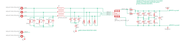
To begin, I am designing a ~3kW phase shifted full bridge design, to take 250VDC to ~1200VDC at ~2.5A. All component selection was based on TI's UCC2895 datasheet.

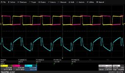
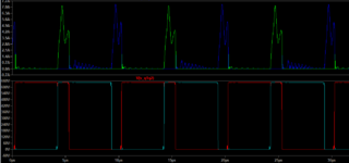
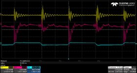
I am experiencing an oscillation in primary current when running the output of my transformer into a rectification stage. When running the mosfet power stage into a resistive load, of a similar power draw, I am not experiencing any oscillation of current. Likewise, when running the mosfet power stage into the transformer, then directly into a resistive load, there are little to no oscillations. My problem only exists while I am running into the rectification stage.

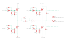
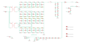
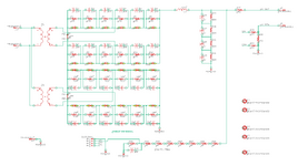
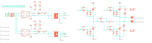
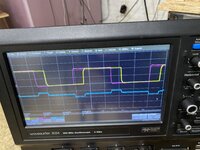
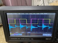
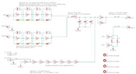
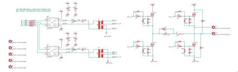
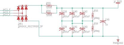
I have attached a picture of the rectification stage to this post - I have since removed the capacitors parallel to the diodes, since I believe my problem to be related to leakage inductance and capacitance on the secondary. I have additionally attached an excerpt of the power stage, as well as scope shots of the bridge current running into a resistive load and into the rectification stage.

I have read through the "Phase Shift Full Bridge SMPS is massively over-hyped" thread, originally posted by treez. One important thing I noticed, is Easy Peasy's suggestion to incorporate a 1nF across the mosfets in the power stage, which I will work to test tomorrow.

I have seen additional designs in which there is an RCD snubber on the output of the rectifier diodes, before the series inductance. I will have to run simulation to find a design that is appropriate.

Aside from these points, is there anything missing I could try?

Thank you
 

Attachments

  • Driver_stage_into_Rectification_stage.JPG
    Driver_stage_into_Rectification_stage.JPG
    4.1 MB · Views: 177
  • Driver_stage_into_load.JPG
    Driver_stage_into_load.JPG
    4.1 MB · Views: 145
  • Driver_stage_into_load.JPG
    Driver_stage_into_load.JPG
    4.1 MB · Views: 128
  • Driver_stage_into_Rectification_stage.JPG
    Driver_stage_into_Rectification_stage.JPG
    4.1 MB · Views: 160
  • 1200V_Rectifier_Stage.JPG
    1200V_Rectifier_Stage.JPG
    76.2 KB · Views: 168
  • 1200V_Power_Stage.JPG
    1200V_Power_Stage.JPG
    44.2 KB · Views: 170
  • 1671486790347.png
    1671486790347.png
    43.7 KB · Views: 189
you got the classic newbie problem of a resonant loop in the output, Lout, C in the diodes, C in the Tx secondary ( in // with the Lsec ), Cout. All the series C ( two paths as CT output ) plus the wiring L for one and via Lout for the other back to the CT.

Really a full bridge of diodes would have been better here - much less volts everywhere, you could also then use a 2 part choke in the + & - to give some CM filtering.

I assume the blue trace is the pri current - since you sort of mention this.

You should be more worried about the PIV across the diodes - if this is OK - then you don't care too much about the current as long as it does not spike up to ridiculous levels.

Can you show the PIV across the diodes ? use two probes and the subtract function on the scope.

Yes, with a lower Lmag ( very small gap in Tx ) and your series choke on the driving side - you can add some C to the fets to limit the dv/dt at turn off - which will help as the sec side ckt will not then get the same "kick" into ringing.

Alternatively placing snubbers across each diode string ( best ) or across the Tx sec's ( 2nd best ) will solve some of the issue of ringing but not the initial current spike. If the freq was low you could use a ferrite bead ( large ammo bead type thing or power ferrite ) in the sec wdg's to each diode to lessen the hit to the diodes and dissipate some of the ringing energy.
--- Updated ---

100kHz may well be too high for 1200V out - as any snubbers will produce a lot of heat .... esp as you have 2 x the output volts and then some on the sec's and diodes ( Psnub ~ C. V^2 Freq )
--- Updated ---

Also you need at least one extra ckt to stop the converter if the output volts go too high ( i.e. for when the the single extant feedback loop fails for any reason ).
--- Updated ---

p.s. congrats that you got this far.
 
Last edited:
I can see that pk curr mode control won't work too well if the CT is in series with the Tx

This is one of those occasions where the CT in line with the DC in looks to be a useful change - albeit limiting the max D to allow reset time on said CT.

What is the decoupling like on the pri side 250V rail ?
 
you got the classic newbie problem of a resonant loop in the output, Lout, C in the diodes, C in the Tx secondary ( in // with the Lsec ), Cout. All the series C ( two paths as CT output ) plus the wiring L for one and via Lout for the other back to the CT.

Really a full bridge of diodes would have been better here - much less volts everywhere, you could also then use a 2 part choke in the + & - to give some CM filtering.

I assume the blue trace is the pri current - since you sort of mention this.

You should be more worried about the PIV across the diodes - if this is OK - then you don't care too much about the current as long as it does not spike up to ridiculous levels.

Can you show the PIV across the diodes ? use two probes and the subtract function on the scope.

Yes, with a lower Lmag ( very small gap in Tx ) and your series choke on the driving side - you can add some C to the fets to limit the dv/dt at turn off - which will help as the sec side ckt will not then get the same "kick" into ringing.

Alternatively placing snubbers across each diode string ( best ) or across the Tx sec's ( 2nd best ) will solve some of the issue of ringing but not the initial current spike. If the freq was low you could use a ferrite bead ( large ammo bead type thing or power ferrite ) in the sec wdg's to each diode to lessen the hit to the diodes and dissipate some of the ringing energy.
--- Updated ---

100kHz may well be too high for 1200V out - as any snubbers will produce a lot of heat .... esp as you have 2 x the output volts and then some on the sec's and diodes ( Psnub ~ C. V^2 Freq )
--- Updated ---

Also you need at least one extra ckt to stop the converter if the output volts go too high ( i.e. for when the the single extant feedback loop fails for any reason ).
--- Updated ---

p.s. congrats that you got this far.

Thank you for your insight, it is greatly appreciated.

Yes, you are correct, blue is primary current (or load current in the case of running directly into resistive load). Purple and Yellow are voltages on each side of the transformer.

100kHz was a educated guess for ideal switching speed, open to criticism on that, and it can be changed. I've never designed a power supply prior to this, and I am aware that 3kW, 100kHz, and 1200V is not an ideal starting point.

Lmag in this case is around 150uH with a <1uH leakage inductance. Going off of what you said, I will add the shim inductance back in and order the 1nF caps for testing.

I will grab scope shots of PIV across one of the diodes and post them today. I can work on simulation and try coming up with a starting point for a snubber circuit.

I can see that pk curr mode control won't work too well if the CT is in series with the Tx

This is one of those occasions where the CT in line with the DC in looks to be a useful change - albeit limiting the max D to allow reset time on said CT.

What is the decoupling like on the pri side 250V rail ?

I am currently planning on running this power supply in voltage control mode, and for testing I am running open loop control of duty cycle. I designed the PSFB controls into an FPGA so they are flexible, and there are means in which I could shoehorn a CT into the design for Pk current mode control.

Decoupling on the 250V rail is 3 sets of 560uF electrolytics in series, with a 2.7uF film capacitor centered and equidistant from each half of the bridge. The reason for the series capacitors; the power stage of this design will likely be modified in the future for higher primary voltages, and I wanted to make it as flexible as possible

I have attached a screen capture of the PCB layout, as well as the schematic. R55 and R56 are bypassed by a relay once the capacitors are charged. The 1Meg resistors are insufficient for this application and I have added additional resistors to bleed off the main caps.
 

Attachments

  • Vbus_filtering.JPG
    Vbus_filtering.JPG
    24.3 KB · Views: 121
  • Rectifier_Stage.pdf
    59.9 KB · Views: 114
  • Rectification_stage.pdf
    52.2 KB · Views: 100
  • Power_stage.pdf
    60.5 KB · Views: 107
  • PCB_layout.JPG
    PCB_layout.JPG
    160 KB · Views: 105
I have some an additional bit of data that I did not think to share earlier, which could be helpful.

I have two transformers that I have been testing with, but both are exhibiting the same problems. The scope screenshots shown earlier are using a 1 : 1.5 : 1.5 transformer of similar specification we had in the shop. The transformer to be used in the final system is a 1 : 6 : 6 ratio (250->1200V).

The reason I am using the 1 : 1.5 : 1.5 transformer at all is because the oscillations are so bad using the 1 : 6 : 6 transformer, it makes the power supply unusable. Using the 1 : 6 : 6 transformer, the supply immediately starts drawing inappropriately high amounts of power at low duty cycles.

Specs for the 1 : 1.5 : 1.5 transformer (designed for 50-100kHz)
- 5.3mH primary inductance
- 12mH secondary inductance (center tap to end)
- 4uH primary leakage inductance
- 16.7uH secondary leakage inductance (center tap to end)
- 370pF capacitance from primary to secondary

Specs for 1 : 6 : 6 transformer (designed for 100kHz, planar)
- 162uH primary inductance
- 5.9mH secondary inductance (center tap to end)
- 0.3uH primary leakage inductance
- 8.8uH secondary leakage inductance (center tap to end)
- 620pF capacitance from primary to secondary

Each transformer was designed by a separate and built by company.

Since I am unable to run the 1 : 6 : 6 transformer at any appreciable duty cycle without damaging mosfets, I ran it at 125V primary voltage, and roughly 15% duty cycle. I have attached a screenshot of the chaos that ensued (IMG_5214). Yellow is one side of the transformer primary, for triggering purposes. Blue and green are each side of a diode in the rectifier stage. Yellow/Gold is the difference between the blue and green traces.

For giggles, I also ran the 1 : 1.5 : 1.5 transformer at 250V primary and took a screenshot (IMG_5215). The results from this transformer are much more in line with expectations. The color coding is the same as above.

In summary
IMG_5214: 1 : 6 : 6 transformer, 125V primary, ~15% duty cycle, 5000 Ohm load
IMG_5215: 1 : 1.5 : 1.5 transformer, 250V primary, ~50% duty cycle, 1000 Ohm load
 

Attachments

  • IMG_5214[1].JPG
    IMG_5214[1].JPG
    4.2 MB · Views: 95
  • IMG_5215[1].JPG
    IMG_5215[1].JPG
    4 MB · Views: 99
Is it simply that the input filter is too high-Q, or the source too inductive (ending up at the same issues & efforts)?

Or, is it that the input filter is doing its job just fine, but that means jamming every bit of displacement current right into measurement ground, and spraying magnetic field out the current loop too?
 
you are missing the resistors on D25, D26, these are generally considered essential.
--- Updated ---

again, for 1200Vout, a full bridge of diodes seems like a better idea, fully utilised Tx, less turns overall, hence less capacitance

Also - planar are bad for capacitance in general.
--- Updated ---

what is the lowest design operating freq for the 1 : 6+6 ?
 
Last edited:
you are missing the resistors on D25, D26, these are generally considered essential.
--- Updated ---

again, for 1200Vout, a full bridge of diodes seems like a better idea, fully utilised Tx, less turns overall, hence less capacitance

Also - planar are bad for capacitance in general.
--- Updated ---

what is the lowest design operating freq for the 1 : 6+6 ?

I currently don't have those diodes installed, since the shim inductor is not installed, but I can make a modification to the board to add in some resistors there.

Thank you, noted, I will work with the manufacturer on a design that is non-planar and designed for full-bridge rectification.

Not sure of lowest design operating frequency - while I was working with the xfmr manufacturer I specified 100kHz with some wiggle room on either end.
 
Usually for step up systems, resonant converters with sine waves across the Tx wdgs are used to reduce the effect of capacitance caused by the higher turns count on the sec's - avoiding sharp edged driving voltages is a good thing in HV design, as high C leads to high current spikes ...

In extreme cases ( EHV ) the sec's are section wound and several transformers may be used to get the desired Vout

e.g. 1kv output windings ( peak ) with 1200V SiC diodes to rectify, thus 5 stages gives 5kV

the primaries are in series usually, but can be in // too, if more than one pri.
--- Updated ---

Referring you your above - the so called series shim inductor is necessary for ZVS at lower loads.
--- Updated ---

50kHz would be considered a high freq for 1200VDC out on a single sec, a good idea to get a transformer done for 50k such that you can try it if 100kHz proves too onerous.

SiC diodes (1200V or 1700V ) are your friends here too, as the rev rec current peaks are way less than for Si diodes.
 
Hello,

jcu85 (original poster) was my coworker and I have picked up the project, and would like to continue seeking advise here.

Since his last post I have made a number of changes, some being from the advise given. Please see the attached schematic of the new output stage. I have replaced the planar transformer with two traditionally wound transformers, with the primaries connected in series and the secondaries both have their own SiC diode full bridges that are combined to produce the output. The switching stage is the same as before but now has the series resistors for D25 and D26 as advised. These are 2.2Ohms (3W).

Note that the transformers I'm currently using for testing are ones we had in house and aren't perfect for our desired output but are close and are good at for our switching frequency. I've measured the following characteristics:

- 154uH primary inductance
- 6.28uH primary leakage
- 5.35mH secondary inductance
- 230uH secondary leakage
- 45pF primary to secondary capacitance <- big improvement here like expected

Here's where I am in testing: A great step in the right direction! The primary current pulses are actually recognizable and power draw has come down a lot as well, and I'm producing pretty stable output at a reasonable level. But the power draw is still high, and it looks to be from these oscillations present between the pulses. The scope shots show the primary current in blue, one at lower output control and one close to the max. I later cranked up the power and ended up destroying diode D25 and its series resistor. The diode failed short and the resistor burned open. I modeled a simulation which revealed large current spikes passing through these diodes between pulses. See attached, blue is I through D25, green is I through D26, red and cyan are voltages across the primaries.

Looking for advise on what might be causing the oscillations and excessive current spikes and what to do about them. Still also very open to criticism and advise on any other design areas as well. Thanks again for the help thus far.
 

Attachments

  • H-Bridge.PNG
    H-Bridge.PNG
    23.3 KB · Views: 84
  • Rectifier Stage.PNG
    Rectifier Stage.PNG
    30.6 KB · Views: 76
  • Shot2.jpg
    Shot2.jpg
    92.5 KB · Views: 73
  • Shot4.jpg
    Shot4.jpg
    89.5 KB · Views: 78
  • D25 D26 I Spikes.PNG
    D25 D26 I Spikes.PNG
    29.5 KB · Views: 85
Hi everyone,

Since last I posted I incorporated much of the advise that was given here and am now in the final strides of completing the first prototype but have run into a few more issues.

Here's what has changed: we have new transformers that were actually designed for the purpose (rather than what was lying around in the shop), transformer primaries are connected in parallel, and I've recalculated a shim inductor value in pursuit of zvs.

During tests I've been finding that the feedback signals for the voltage and current from the output stage were appearing incredibly noisy on the scope with intense spikes and ringing that occur periodically at the switching frequency. I investigated further and suspect that switching noise must be getting to the scope through line or ground as the noise was present even when the scope probes were not connected anywhere on the supply. Should I be reworking my input filter to try and combat this or is this common with high power switch mode supplies?

I was hoping for advise on determining switch dead time to optimize zvs if available. I've found a number of papers and other sources detailing the process but they seem to all have a different approach that each land me at a different answer. I took a stab in the dark at this and while my shim inductor seems to be doing it's job, the switching losses are still through the roof. MOSFETs are failing at about half power.

Lastly, during testing I've found that my output power is coming up shorter than expected. I'm thinking that a big contributor might be the switching losses mentioned before but would greatly appreciate any critique on that assumption.

I've attached some updated schematic images and scope image where red and yellow are feedback samples and blue is current through the transformer primaries.

Thanks again for all the previous help. Try not to laugh too hard at my newbie struggles here, this is my first switching supply design and picking up in the middle of an already partially developed project has had some interesting challenges.
 

Attachments

  • Shot1.jpg
    Shot1.jpg
    74.1 KB · Views: 53
  • Input Stage.PNG
    Input Stage.PNG
    15.2 KB · Views: 48
  • Output Stage.PNG
    Output Stage.PNG
    30.4 KB · Views: 46
  • Switching Stage.PNG
    Switching Stage.PNG
    23.1 KB · Views: 58
your 2R2 resistors are too small - replace with 22 ohms, this will remove a lot of the switching noise - you can optimise later

are your fets heatsunk to an earthed heatsink ?

do you have pictures of the gate drive and surrounding layout ?
--- Updated ---

Also - you still have not shown pictures of the de-coupling near the main mosfets - the root cause of much of the ringing.
 
Last edited:

LaTeX Commands Quick-Menu:

Similar threads

Part and Inventory Search

Welcome to EDABoard.com

Sponsor

Back
Top