Continue to Site

Welcome to EDAboard.com

Welcome to our site! EDAboard.com is an international Electronics Discussion Forum focused on EDA software, circuits, schematics, books, theory, papers, asic, pld, 8051, DSP, Network, RF, Analog Design, PCB, Service Manuals... and a whole lot more! To participate you need to register. Registration is free. Click here to register now.

Problem with Power H-Bridge

Status
Not open for further replies.

Matinking

Newbie level 4
Joined
Jun 13, 2013
Messages
6
Helped
0
Reputation
0
Reaction score
0
Trophy points
1
Activity points
50
Hi Everybody!
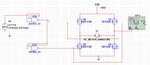
I am going to design a mosfet-based power H-bridge with below properties : 100V, 10A

I've opted the NPN transistors as IRF530N. working frequency is rather 50kHz and the applied PWM wave is in the range of 0-5.
I did the simulation in the NI Multisim 11.0......
I have terrible outputs in the output terminals of the circuit.... As I should see switching in the terminals between 100V and -100V, the voltage of the two terminals is just 1.039v!!!!!!!!!!!!!!!!!!!!!!!!!!!!!

Does anybody help me to resolve the problem???

Attached files are the circuit picture and the project file in NI Multisim 11.0.

Thank you
 

Attachments

  • Untitled.jpg
    Untitled.jpg
    195.8 KB · Views: 107
  • Design4.7z
    496.9 KB · Views: 65

You are missing level-shifting gate drivers for the high side transistors. Also CD4011 isn't suited as low side gate driver for 50 kHz.
 

You are missing level-shifting gate drivers for the high side transistors. Also CD4011 isn't suited as low side gate driver for 50 kHz.

hey

Actually I would like to add that gate drivers into the circuit, the drivers like LCI7667, but the driver modules of the Multisim 11.0 are terribly poor.
there is just a rear models of the drivers like UCC and TPS family.
Is there any way to resolve this problem without switching the simulator??

by the way, Would you please guide me to choose the desired operating frequency for the system?

Thank you
 

What's the simulaton purpose?

If you want to evaluate real hardware behaviour (e.g. switching speed, losses), you need realistic driver models. For a simple functional simuation, you can use controlled voltage sources as driver replacement.
 

What's the simulaton purpose?

If you want to evaluate real hardware behaviour (e.g. switching speed, losses), you need realistic driver models. For a simple functional simuation, you can use controlled voltage sources as driver replacement.

Yes...

That must be entirely an empirical circuit for driving of the DC motors mounted on a huge manipulator......
So, you mean that I have to change the simulator to access to the desired systems...right?
 

Multisim is SPICE and can read generic SPICE models. In so far there's no need to change the simulator, as long as you are satisfied with it's features and performance in general.

Another question is how we rate the project's chances for success without substantial experience in the power electronics field.
 

Hello Matinking,

Well there are a number of issues that I can see before evening begining to consider any basic calculations. If memory serves an IRF530 will have a threshold voltage or around 5V so your 5V nand inverters are going to hardly even be able to drive your devices into an on state.

Secondly, you need to consider the drive current needed to quickly charge and discharge the gate capacitance. I doubt your logic gates will have enough instantaneous current drive to achieve this. This is a combination of the gate to source capacitance and the gate to drain capacitance which will become much larger due to the miller effect over a 100V range! The total current you need to source and sink will be the total current to charge and discharge these capacitors. You will also want to be able to charge and discharge these capacitance about 100 times faster than the period of your 50KhZ signal.

Finally, you need to ensure that you have a more concrete non overlap between turning the top transistor off when the bottom transistor is on other wise you will have current shoot through and will burn out your bridge. Power driver circuits require a little more consideration, you could consider a non overlapping clock architecture but you need to consider level shifting and high current drive stages.

Hope this helps, best wishes, Ken.
 

Hello Matinking, your mosfets behave like NPN transistors, except that you need to drive them with a higher voltage between gate and source. Q1 and Q3 you can see as emitter followers (now Source followers). If you want to drive the source to 100V, you need about 108V between gate and ground. your logic gates only provide 5V.

You can be happy that there are special H-bridge drivers that do everything for you (avoiding cross conduction (that is Q1 and Q2 both on, resulting in smoke), providing high voltage for driving the upper transistors, and they provide the drivers itself to charge and discharge the gate-source capacitance very fast).

Though you may directly drive the motor, you will likely produce lots of RF interference that may even affect FM radio reception. To avoid this, you need to filter the output. If the motor can behave as a generator, you need provisions to dissipate the energy delivered back by the motor. One solution can be a self-locking worm gearbox, but that reduces efficiency.

Is this just for a study, or real design? Design and actual construction of 100V/10A will be very hard (to impossible) without an experienced person around you. Due to the power, if things go wrong, they can go really wrong.
 
Status
Not open for further replies.

Similar threads

Part and Inventory Search

Welcome to EDABoard.com

Sponsor

Back
Top