Continue to Site

Welcome to EDAboard.com

Welcome to our site! EDAboard.com is an international Electronics Discussion Forum focused on EDA software, circuits, schematics, books, theory, papers, asic, pld, 8051, DSP, Network, RF, Analog Design, PCB, Service Manuals... and a whole lot more! To participate you need to register. Registration is free. Click here to register now.

Problem with my h-bridge circuit

Status
Not open for further replies.

SVS1988

Newbie level 3
Joined
Feb 10, 2014
Messages
3
Helped
0
Reputation
0
Reaction score
0
Trophy points
1
Activity points
22
Hi everyone,

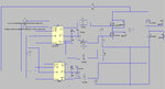
I designed a H bridge circuit and I have attached the circuit.
The circuit s motive is to convert 300 v D C into pulsed DC at various frequency levels (10-60KHz).

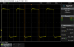
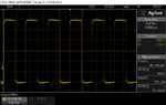
so, first i divided the circuit into two half bridges and i tested both the halves independently.
it worked perfectly . No error .(See the attached scope)

But now when i drive the whole h bridge circuit , I get noise and distortion after 35-40 Volts.
what could be my problem?

Thank you !
 

Attachments

  • H_bridge circuit.jpg
    H_bridge circuit.jpg
    459.4 KB · Views: 91
  • scope _300 V_20khz.png
    scope _300 V_20khz.png
    22.6 KB · Views: 86
  • scope _300 V_30khz.png
    scope _300 V_30khz.png
    23.5 KB · Views: 76

I am sure that problem is input, output capacitances of MOSFET.
Change your MOSFET! Take less powerful (you have just only 0,3A)
 

I am sure that problem is input, output capacitances of MOSFET.
Change your MOSFET! Take less powerful (you have just only 0,3A)

This is just a test circuit. In the future i will be having a inductive load and the current flowing will be approximately 3-4 Ampere.

if Input output capacitance of the MOSFET is the problem, then how did the half bridge circuit work?

Thank you!
 

what could be my problem?
E.g. bad circuit layout, insufficient DC-bus capacitors, output stage crosstalk to gate control signals
 

E.g. bad circuit layout, insufficient DC-bus capacitors, output stage crosstalk to gate control signals

can you please be specific??
 

Could you just change load (R with 100 Om) and to show your result.
And FvM is right, DC-bus capacitance must be.
 

The output contains a high frequency voltage superimposed on the DC voltage. This suggests oscillating components in the signal or/and power path.
1. What is the distance between the MOSFET driver and the MOSFET? At high frequencies, a few centimeters long wire can cause a noticeable oscillation due to parasitic inductance of the wire.
2. The driver should be placed as close as possible to the MOSFET.
3. Use thinner signal wire to reduce parasitic inductance.
 

can you please be specific??
I mentioned several problems that are often observed in MOSFET bridges.

You didn't give substantial informations about your design except for showing a (simulation) circuit.
No, I can't be presenly more specific.
 

Status
Not open for further replies.

Part and Inventory Search

Welcome to EDABoard.com

Sponsor

Back
Top